P1-6 / S. Lee
• IMID 2009 DIGEST
Abstract
Phosphorus doped ZnO (PZO) thin films were deposited on SiO2/n-Si substrates using DC magnetron sputtering system varying oxygen partial pressures from 0 to 40 % under Ar atmosphere. The deposited films showed reduced n-type conductivity due to the compensating donor effects by phosphorus dopant. The bias-time stability shows relatively good stability over bias and time comparing to un-doped ZnO-based TFTs
1. Introduction
Amorphous silicon (a-Si) is widely used for the commercial display’s channel layer (1). Due to its limitation on mobility (< 1 cm2/Vs), there have been searching for new materials. In recent years, researches on oxide materials are being carried out because of their high electron mobility and other interesting characteristics such as transparency, flexibility. However, it is difficult to achieve p-type conductivity in oxide materials due to the self-compensating effects by intrinsic donor defects and low solubility of the p-type dopants such as N, P, and As (2-3). Thus, this should be a hurdle in developing pn-junction and CMOS using the transparent and flexible oxide materials. The aim of this study is to adjust n-type conductivity using a p-type dopant and finally to suggest a way to obtain stable p-type conductivity.
2. Experimental
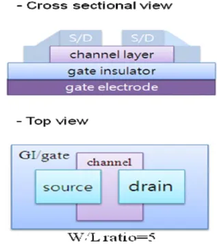
Phosphorus doped Zinc oxide TFT unit cells were fabricated on a heavily doped n-type silicon substrate on which SiO2 with thickness of 100 nm was thermally deposited. As shown in Figure 1, the TFTs cells with a bottom gate structure had the doped substrate as a gate and the SiO2 layer as a gate insulator. A sintered mixture of 99.99 % pure ZnO and
3 wt% 99.99 % P2O5 was used to deposit the PZO channel layers of the TFTs using DC magnetron sputtering system. The channel layers were deposited under Ar atmosphere varying oxygen content percentage from 0 % to 40 %. The substrate temperature was set to be 100 °C and the plasma discharge power density was adjusted to be 0.5 W/cm2. The thickness of the deposited channel layers was approximately 100 nm.
Fig. 1. Cross sectional and top view of the PZO-TFT device
Indium tin oxide films used as source and drain electrodes of the TFTs were deposited on the channel layers at room temperature by the DC sputter. The thickness of electrodes was fixed to be 300 nm. The channel layers and the source and drain electrodes were patterned by using shadow masks.
The electrical properties of the PZO channel layers
Characteristic of P doped ZnO-based thin film transistor by DC
magnetron sputtering
Sih Lee
1, Yeon-Keon Moon
1, Dae-Yong Moon
1, Woong-Sun Kim
1,
Kyung-Taek Kim
1, and Jong-Wan Park
11
Dept. of Materials Science and Engineering, Hanyang University, Seoul, Korea
Tel.:82-2-2220-0386, E-mail: [email protected]
P1-6 / S. Lee
IMID 2009 DIGEST • were analyzed using Hall Effect measurement system
(Ecopia, HMS-3000); carrier concentration and resistivity of the channel layers were measured through van der pow method. Current-voltage characteristics of the PZO-TFTs were taken by a semiconductor parameter analyzer (HP 4145B) in the dark.
3. Results and discussion
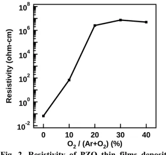
Phosphorus doped ZnO (PZO) thin films were deposited on SiO2/n-Si substrates using DC magnetron sputtering system. The films were deposited in argon atmosphere varying oxygen partial pressures from 0 to 40 %. The structural and electrical properties of pristine and thermally treated PZO thin films were examined. The films showed reduced n-type conductivity due to the compensating donor effect by phosphorus dopant. It is shown in figure 2.
10-2 100 102 104 106 108 Re si s ti v ity (o h m -c m) 40 30 20 10 0 O2 / (Ar+O2) (%)
Fig. 2. Resistivity of PZO thin films deposited with various oxygen partial pressures.
The resistivity of the PZO films shows dependence on oxygen partial pressures up to a certain point.
As shown in figure 3 and table 1, the current voltage curves of TFT unit cells were obtained with HP4145 semiconductor analyzer and exhibited proper transfer and output characteristics with good stability. The bias-time stability test was also conducted to the TFT unit cell, which shows relatively good stability over bias and time comparing to un-doped ZnO-based TFTs that were previously studied.
10-11 10-9 10-7 10-5 10-3
Drain Current, I
d(A)
-40 -30 -20 -10 0 10 20 30 40Gate-Source Voltage (V)
Vds=10 V 10 % 20 % 30 % 40 %Fig. 3. Transfer characteristic curves of TFTs with channel layers deposited in various oxygen partial pressures .
TABLE 1. characteristic parameters of TFTs with channel layers deposited in various oxygen partial pressures.
O2
/(Ar+O2) Von (V)
μFE
(cm2/Vs) (V/dec) S
10 % N/A N/A N/A
20 % -3 1.61 1.94
30% 7 0.18 3.84
40 % 2 0.12 4.73
4. Summary
This research studied phosphorus doped ZnO based thin films and the transistors with the channel layers using the films.
N-type conductivity of the ZnO film was controlled using a p-type dopant and was comparatively more stable than the un-doped ZnO films. This suggests a way to obtain stable p-type conductivity provided that the solubility of p-type dopant is enhanced.
P1-6 / S. Lee
• IMID 2009 DIGEST
Acknowledgement
This work was supported by the Korea Research Foundation Grant funded by the Korean Government (MOEHRD) (KRF-2007-313-D00453).
5. References
1. J. F. Wager, D. A. Keszler, and R. E. Preseley, Transparent Electronics (Springer, New York, 2008).
2. J. Nause, M. Pan, V. Rengarajan, S. Ganesan, A. Payne, N. Li, L. Ferguson, SPIE 70, 5941 (2005). 3. Z. Ye, W. Xu, Y. Zeng, J. Liu, B. Zhao, L. Zhu, J.
Lü, L. Wang, X. Li, Chin. J. Semicond. 26, 2264 (2005).