P2-92 / M. H. Ahn
• IMID 2009 DIGEST
Abstract
For the application of flexible substrate to future display and new transparent devices, indium tin oxide (ITO) thin film was formed on polycarbonate(PC) substrate at room temperature by in-line sputter system. During the ITO sputtering, Ar and O2 reaction gas were fixed at a constant value and the process pressure was varied from 3 to 7 mtorr. From the electrical and the optical properties of sputtered ITO films, the sheet resistances of as-deposited ITO films varied with a different pressure and the optical transmittances of the ITO films at visible wavelength were maintained above 85%. The results are considered to be due to the saturation of O2 atoms from reaction in ITO film.
1. Introduction
Transparent and conductive indium-tin oxide (ITO) film is a highly degenerated wide gap semiconductor that is commonly used as transparent electrodes in flat panel display, such as liquid crystal displays (LCD), touch panel, plasma display panels (PDP) and organic light emitting diodes (OLED) on account of its high transparency in the visible region and low resistivity. The ITO films have been deposited by various methods, such as chemical vapor deposition, sol–gel, evaporation and sputtering, etc. As a method of sputtering, DC magnetron sputtering is the most attractive process in terms of industrial productivity due to its potential for homogeneous large-area coating, good reproducibility and high deposition rate. [1-4]
Recently, ITO electrode has attracted much attention in flexible electro-optical devices because of their merits such as light weight, durability, flexibility, and durability. Especially, it is necessary to deposit ITO film at room temperature on flexible substrate because the substrate cannot bear up against the high temperature processes. In the manufacturing processes of optoelectronic devices, a lot of attempts are carried
out about the ITO deposition at room temperature [5-9]. However, it is still difficult to use polymer substrates in sputtering processes or post annealing treatments due to their low thermal resistance and high thermal expansion.
In our study, we selected polycarbonate(PC) as the substrate because of its thermal resistance and mechanical, electrical properties and sputtered the ITO film on the PC film at the room temperature using in-line DC magnetic sputtering system.
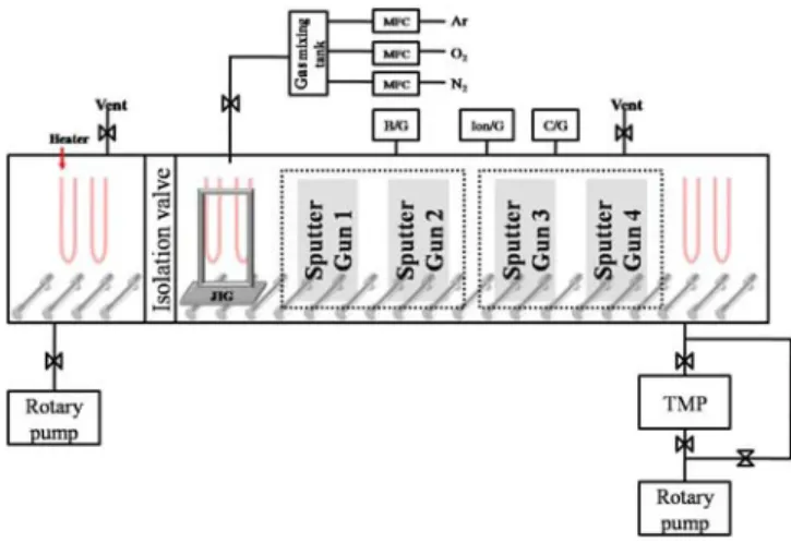
Fig. 1. Schematic of the in-line sputtering system used in the experiment
2. Experimental
ITO thin films were deposited on PC substrate by in-line DC magnetron sputtering. An ITO target was composed of the sintering of In2O3 (90 wt%) and
SnO2 (10 wt%). Figure 1 shows the schematic of the
in-line sputtering system used in the experiment. The PC substrate was stuck on the 370×470×1 mm3
soda-lime glass and was stood up vertically in the sputter system. During in-line sputtering, the substrate was
ITO Thin Film Deposition on Polycarbonate Substrate using
In-Line DC Magnetron Sputtering
Min Hyung Ahn, Zhao-Hui Li, Kyung Min Choi, Seung Hyeok Im,
Kyung Seo Jung, Eou Sik Cho, and Sang Jik Kwon
a*
Department of Electronics Engineering, Kyungwon University, San 65,
Bokjung-dong, Soojung-gu, Seongnam, Kyunggi 461-701, Korea
Phone: +82-31-750-5319 , E-mail: [email protected]
P2-92 / M. H. Ahn
IMID 2009 DIGEST •
moved at a speed of 30~150 cm/min.
Prior to sputtering, the process chamber of in-line sputter was evacuated to a pressure of 1×10⁻⁶ torr.
Then high-purity Ar and O2 gas were injected into
process chamber through a mass flow controller (MFC) at flow rate of 50 sccm and 2.5 sccm, respectively. The ITO target was pre-sputtered for 3 minutes for the removal of the impurities from surface of ITO target.
In this experiment, the ITO film was deposited with a variety of sputtering pressure. Table 1 shows the deposition conditions.
TABLE 1. Deposition condition of ITO films.
Sputter condition Value DC power 1.5 kW Base vacuum 1×10⁻⁶ torr
O2 gas flow rate 2.5 sccm Ar gas flow rate 50 sccm Moving speed of substrate
during sputtering 120 cm/min Sputtering pressure 3~7 mtorr After deposition, the thickness of the ITO film was measured with a surface profilometer (alpha-step 500, Tencor), and the sheet resistance was measured by a 4-point probe (CMT-SR2000N, AIT). The transmittance was analyzed using a UV-Vis spectrometer(Cary100, VIRIAN) from 200 nm to 800 nm.
3. Results and discussion
When a plasma occurs in the process chamber of the DC magnetic sputtering system, the Ar gas and the O2 gas were separated into Ar+ or O+ ions, respectively.
These ions are accelerated by the electrical field caused by the magnetron so that they make collisions to the substrate, the depositing ITO film. As the Ar+ or
O+ ions play important roles in sputtering, we made
ITO deposition with various sputtering pressure and analyze the electrical and optical properties of the ITO films.
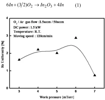
Figure 2 shows the sheet resistances (Rs) of ITO
thin film sputtered with various pressures. From 3 mtorr to 4 mtorr, the sheet resistance of ITO film decreased with the sputtering pressure increasing. However, the sheet resistance increases with the sputtering pressure above 4 mtorr.
Fig. 2. Sheet resistance of ITO film sputtered with various pressures.
During ITO sputtering process, the oxygen element may be insufficient in the formation of ITO film on PC substrate and InO, SnO oxides may be formed in ITO films. As a result of the low quality oxide and In or Sn element without oxygen in ITO film, the electron concentration of ITO film decreases and the electron mobility also decreases. Ultimately, the sheet resistance of ITO film increases. The following formula shows the chemical reaction in the ITO film when the oxygen element is insufficient.
In O In O In (3 2) 4 6 + 2 → 2 3+ (1)
Fig. 3. The uniformity in sheet resistance of ITO film sputtered with various pressures.
P2-92 / M. H. Ahn
• IMID 2009 DIGEST
supplementary oxygen element from O2 gas was so
deficient that the sheet resistance of ITO film was increased. On the other hand, the redundant oxygen element exits from the ITO film at the pressure above 5 mtorr and the sheet resistance increases with the increasing of the sputtering pressure.
The uniformity in sheet resistances of the ITO film sputtered with various pressures was shown in Fig. 3. The Rs uniformity was fluctuated in a range of 1~3 %
at the substrate size of 370×470 mm2. It means that the excellent uniform ITO film was obtained.
Fig. 4. Thickness of ITO film sputtered with various pressures.
Fig. 5. Transmittance spectrum of ITO film sputtered with various pressures.
Thickness of ITO film sputtered with various
pressures was measured as shown in Fig. 4. It is clear that the thickness of ITO film increases with the pressure increasing. It shows that the sputtering rate also increases with the pressure increasing. Therefore, it is possible to consider the relationship between the content of oxygen and the composition of ITO film.
Figure 5 shows the transmittance of ITO film sputtered with various pressures. In spite of the variable sputtering conditions, the ITO films have similar transmittances above 85 % at the visible range of wavelength (400~800 nm).
Fig. 6. Transmittance at 550 nm of ITO film sputtered with various pressures.
The transmittance at 550 nm of ITO film was shown in Fig. 6. As mentioned above, the transmittance of the ITO film had a little fluctuation with the variation of deposition pressure. The transmittance of all the ITO film was above 85%.
4. Summary
ITO thin films were deposited on polycarbonate substrate using in-line DC magnetic sputtering system with various pressures at room temperature. The experimental results showed that the sheet resistance and the thickness of ITO film varied with different deposition pressure. The minimum sheet resistance (320 Ω/□) was obtained when the pressure was 4 mtorr. However, the thickness and the deposition rate were increased with the increase of deposition pressure. Otherwise, the transmittance of ITO film is over 85%, and it has little fluctuation with the variation of deposition pressure.
P2-92 / M. H. Ahn
IMID 2009 DIGEST •
Acknowledgements
This work was supported by GRRC (Gyeonggi Regional Research Center) at Kyungwon university.
5. References
1. B. S. Chiou and S. T. Hsieh, Thin Solid Films, 229, 146 (1993).
2. B. S. Chiou, S. T. Hsieh and W. F. Wu, J. Am.
Ceram. Soc., 77, 1740 (1994).
3. J. A. Dobrowolski, F. C. Ho, D. Menagh, R. Simpson and A. Waldorf, Appl. Opt., 26, 5204 (1987).
4. A. Kulkarni, T. Lim, M. Khan, and K. Schilz, J. Vac.
Sci. Technol., A16, 1636, (1998).
5. T. karasawa and Y. Miyata, Thin Solid Films, 223, 135 (1997).
6. P. Lippens, A. Segers, J. Haemers, R. De Gryse,
Thin Solid Films, 317, 405 (1998).
7. W. Wu and B. Chiou, Thin Solid Films, 298, 221 (1997).
8. T. Minami, H Sonohahra, T. Kakumu, and S. Takata,
Thin Solid Films, 270, 37 (1995).
9. N. Danson, I. Safi, G. Hall and R. Howson, Surf.