1. 서 론
현재 세계 디스플레이 사업 동향은 고화질화, 대형 화 쪽으로 흘러가고 있고 이에 발맞춰 많은 회사들은 보다 수준 높은 디스플레이 기술을 개발하기 위해 LCDs, OLEDs, PDP를 구성하는 투명전도막(transparent conducting film) 분야의 연구를 진행하고 있다. 때문
a. Corresponding author; [email protected]
Hee-Joon Jang, Han-Joon Yoon, and Gyeong-Nam Lee equally contributed to this work.
Copyright ©2018 KIEEME. All rights reserved.
This is an Open-Access article distributed under the terms of the Creative Commons Attribution Non-Commercial License (http://creativecommons.org/licenses/by-nc/3.0) which permits unrestricted non-commercial use, distribution, and reproduction in any medium, provided the original work is properly cited.
에 이를 구성하는 투명전극에 대한 관심도가 높아지는 것은 자연스러운 현상이라고 할 수 있다. 디스플레이에 사용할 수 있는 투명전극을 판단하는 기준은 광 투과율 과 전기 전도성이다. 400~800 nm의 가시광선 영역에서 투과율이 80% 이상이어야 하고 비저항이 10
cm 이 하여야 한다. 지금까지 이에 가장 적합하다고 판단되는 산화물이 ITO (indium tin oxide)와 AZO (aluminum zinc oxide)이다 [1,2].ITO는 3.5~4.3 eV의 큰 밴드 갭을 갖는 N-type 전 도성물질로서 가시광선 영역의 빛 파장을 통과시켜 광 학적 투명성, 높은 전기 전도도를 가지고 있는 것이 특징이다 [3]. 그러나 ITO는 저온에서 증착을 하는 데 어려움이 있고, 산소나 수소의 플라즈마를 이용해 ITO 를 스퍼터링(sputtering) [4-6] 할 때 음이온들 간의
ITO/AZO 투명전극을 이용한 Si 기반의 광전소자
장희준1, 윤한준1, 이경남1,2, 김준동1,2,a
1 인천대학교 전기공학과
2 인천대학교 차세대 융합에너지연구소 광전에너지소자연구실
Si Based Photoelectric Device with ITO/AZO Double Layer
Hee-Joon Jang
1, Han-Joon Yoon
1, Gyeong-Nam Lee
1,2, and Joondong Kim
1,2,a1 Department of Electrical Engineering, Incheon National University, Incheon 22012, Korea
2 Photoelectric and Energy Device Application Lab, Multidisciplinary Core Institute for Future Energies, Incheon National University, Incheon 22012, Korea
(Received December 11, 2017; Revised January 11, 2018; Accepted January 12, 2018)
Abstract: In this study, functional transparent conducting layers were investigated for Si-based photoelectric applications.
Double transparent conductive oxide (TCO) films were deposited on a Si substrate in the sequence of indium tin oxide (ITO) followed by aluminum-doped zinc oxide (AZO). First, we observed that the conductivity and transparency of AZO dominate the overall performance of the double TCO layers. Secondly, the double layered TCO film (consisting of AZO/ITO) deposited by sputtering was compared to a AZO-only film in terms of their optical and electrical properties.
We prepared three different AZO films: ITO:3min/AZO:10min, ITO:5min/AZO:7min, and ITO:7min/AZO:4min. The results show that the optical properties (transmittance, absorbance, and reflection) can be controlled by the film composition. This may provide a significant pathway for the manipulation of the optical and electrical properties of photoelectric devices.
Keywords: ITO, AZO, Transparent conductive oxide (TCO), Si, Photoelectric devices
ISSN 1226-7945(Print), 2288-3258(Online)
충격으로 인해 ITO의 박막에 손상이 일어나 전기적 특 성이 감소하게 된다. 동시에 저항이 증가하게 되면서 투명전극의 효율이 떨어지게 된다는 문제점을 안고 있 다 [7]. AZO는 에너지 밴드 갭이 3.37 eV인 TCO 물 질로써 낮은 비저항을 가지고 ITO와 마찬가지로 가시 광선을 잘 통과시킨다. 높은 광학적 특성과 전기 전도 도를 가지고 있는 N-type 투명전극과 결합해 높은 효 율을 보일 가능성이 매우 큰 우수한 물질이다. 또한 AZO 박막은 저온 증착에서 높은 성장을 가지는 물질 중 하나이다 [8,9]. 따라서 ITO와 AZO를 적절히 배합 한다면 ITO의 단점을 보완함과 동시에 ITO/AZO의 광 전자 반응 [10], 반사율/투과율/흡수율 [11]을 개선하 여 더욱 우수한 전기적/광학적 특성을 갖는 물질을 만 들 수 있다.
본 실험에서는 Al (aluminium)과 N-type 실리콘이 결합된 기판 위에 ITO를 3분, 5분, 7분 동안 증착시킨 다음, ITO 기판 위에 AZO를 10분, 7분, 4분 동안 증 착한 AZO 기판을 결합하였다. 이렇게 본 실험에 사용 할 전극 모델로 ITO/AZO 기판의 두께가 30 nm/70 nm인 No.1 Device, 두께가 50 nm/50 nm인 No.2 Device, 마지막으로 두께가 70 nm/30 nm인 No.3 Device를 만들었다. ITO/AZO를 결합한 3가지 전극들 을 실험함으로써 물질의 투명전극 효율성 및 전기적/
광학적 특성을 비교 분석하였다.
2. 실험 방법 2.1 실험 방법 및 순서
본 실험에서는 n-Si 기판을 사용해 차례로 100 nm 두께의 AZO와 50 nm 두께의 ITO를 sputtering을 하
였고 기판을 뒤집어 Al을 후면 전극으로 사용하였다.
그리고 ultrasonic cleaner를 이용하여 아세톤, 메탄 올, 증류수 순서로 세정을 하였으며, 건조 작업으로 nitrogen blowing을 하였다. 실험의 공정 순서는 그림 1에 나타내었다. n-Si의 기판 위에 RF 스퍼터링 방식 을 이용하여 working pressure을 5 mtorr, RF 300 W으로 AZO 필름을 증착하였다. 그 위 같은 조건에서 DC 스퍼터링 방식을 이용하여 ITO 필름을 증착한 후 550℃에서 RTP 열처리 과정을 10 min 간 진행하였 다. Al을 DC 스퍼터링을 이용하여 증착한 후 마지막으 로 RTP 열처리 과정을 함으로써 투명전극의 저항 값 을 낮추고 투과성을 증가시켰다. 일반적으로 TCO 물 질은 후열처리를 통해 투과성과 전도도를 개선시킬 수 있다.
이번 실험의 반도체 소자 구조를 관찰하기 위해서 전계 방출형 주사 현미경(FE-SEM)을 사용하였고, 3개 의 반도체 소자의 전기적/광학적 특성을 비교 및 분석 하기 위해 UV-vis spectro photometer를 사용하여 투과율, 흡수율 그리고 반사율을 측정하였다. 마지막으 로 광 응답 비를 구하기 위해, 광 응답 장비(WonA, ZIVE SP1)을 사용하였다.
3. 결과 및 고찰
그림 2(a), (b)에서는 RTP 열처리 후의 No.2 소자의 SEM Images를 보이고 있다. 그림 2(c)는 실제 소자의 사진을 보이고 있다. SEM-images를 통해 각각 50 nm 두께의 ITO, AZO층을 얻었으며 Si 기판 위에 AZO와 ITO가 증착되었음을 확인하였다.
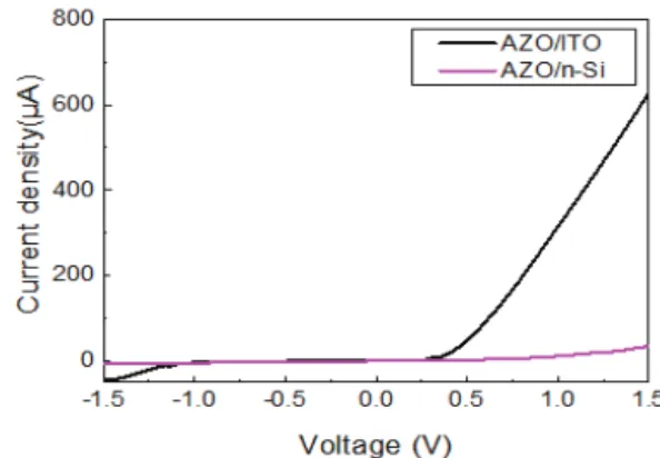
표 1에는 각 소자의 sheet resistance 값을 나타내었 다. ITO의 두께가 증가할수록 투명전극의 sheet resis- tance 값이 줄어들었고 RTP 열처리 후에는 약 68, 32, 20 /□의 수치가 측정되었다. 그림 3은 AZO 단 일층 소자와 ITO를 이용한 복합층 소자의 Dark Ⅰ-Ⅴ 특성 그래프이다. AZO/n-Si와는 달리 ITO/AZO를 이 용한 소자에서는 정방향 전압에서 전류가 급격히 증가 하는 특성을 보여주고 있다. 이는 ITO의 사용으로 저 항을 크게 개선시킨 결과에 의한 것으로 볼 수 있다.
따라서 AZO만 있는 것보다 ITO/AZO 결합이 된 반도 체가 전극으로 더욱 우수한 성능을 제공할 수 있는 것 으로 판단된다.
그림 4에서는 ITO/AZO/n-Si 광전소자의 광학적 특 성을 나타내었다. ITO/AZO 투명전극은 단파장을 제외 Fig. 1. Fabrication steps of photoelectric device.
(a)
(b)
(c)
Fig. 2. FE-SEM images (a) cross-section, (b) top-view, and (c) schematic and photogragh of No.1/No.2/No.3 devices.
Fig. 3. Dark Ⅰ-Ⅴ Characteristic AZO/n-Si/AZO/ITO.
(a)
(b)
(c)
Fig. 4. Optical properties (a) transmittance, (b) absorbance, and (c) reflectance.
AZO/n-Si ITO/AZO/n-Si After RTP process No.1 device 71.08 k/□ 275.43 /□ 68.74 /□
No.2 device 83.27 k/□ 104.23 /□ 32.18 /□
No.3 device 94.56 k/□ 45.23 /□ 20.24 /□
Table 1. Sheet resistance of AZO/ITO/AZO-ITO deposition.
한 영역에서 80% 이상의 높은 투과율을 가지고 단일 AZO층과 비교하여 비슷한 반사율을 보여주고 있다.
ITO층의 사용은 소자에 광학적으로 손해를 주지 않는 다는 것을 의미한다. ITO/AZO 투명전극의 높은 투과율 로 인해 흡수층인 Si에 충분한 빛이 도달할 수 있도록 할 수 있고 이는 광전소자의 성능에 큰 영향을 미치는 요인이라고 할 수 있다. 또한 투명전극은 Si의 높은 반 사율을 저감시켜 주는 ARC (anti-reflection coating)의 역할을 수행할 수 있다.
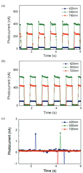
접합소자의 성능을 알아보기 위해 photocurrent 값 을 측정하였다. 그림 5는 각 소자의 광 응답을 나타내고 있으며 광전류는 표 2에 나타내었다. 각 소자의 광전류 는 No.1 소자에서 21.7, 387, 221 nA, No.2 소자에서 103, 646, 446 nA의 수치가 420, 560, 740 nm의 파장 순으로 측정되었다. 특히 560 nm의 파장에서 가장 큰 광전류가 측정되었고 이는 흡수층으로 사용된 Si의 특성 에 의한 것으로 Si 기반의 광전소자는 약 500~600 nm 의 파장에서 가장 큰 출력을 가지기 때문이다 [12]. 각 소자는 ITO층의 증가에 따라 광전류의 수치도 증가하였 고 이는 ITO층으로 인한 sheet resistance 감소의 영향 으로 분석된다. 하지만 No.3 소자에서는 광전류가 측 정되지 않았다. 이는 가장 두꺼운 ITO층으로 인해 저 항의 수치는 최저를 보였지만 접합층으로 사용된 AZO 의 두께가 너무 얇아 Si과의 접합이 제대로 이루어지 지 않았다고 볼 수 있다 [13].
4. 결 론
본 연구에서는 스퍼터링을 이용해 ITO/AZO를 n-Si 기판에 각기 다른 두께로 증착시켜 세 가지의 광 검출 기 소자를 제작하였다. 이를 토대로 전기적/광학적 특 성을 비교 분석하여, 투명전극으로서의 활용성에 대해 실험 및 분석을 하였다. 세 가지 device는 모두 다른 sheet resistance (68.74 /□, 32.18 /□, 20.24
/□) 값을 갖고 있지만 가시광선 영역을 포함하여 전 파장에서 대략 80%의 높은 투과율을 관찰할 수 있었 다. 그에 반해 반사율은 30% 이하의 낮은 값을 얻을 수 있었다. 각 device의 광전류는 420, 560, 720 nm 파장에서 ITO를 50 nm, AZO를 50 nm의 두께로 증 착시켜 스퍼터링한 No.2 소자가 가장 높은 광전류를 보였다. 위의 요소들을 바탕으로 투명반도체 소자의 전 기적/광학적 특성을 활용하면 ITO/AZO가 고성능 투 (a)
(b)
(c)
Fig. 5. Photo response (a) No.1 device, (b) No.2 device, and (c) No.3 device.
Photocurrent (nA)
420 nm 560 nm 740 nm
No.1 device 21.7 387 221
No.2 device 103 646 446
No.3 device - - -
Table 2. Photo and dark current of No.1/No.2/No.3 device.
명전극과 광전소자 기술 분야에 있어 긍정적인 영향을 끼치게 될 것이라고 판단된다.
감사의 글
The authors acknowledge the financial support of Basic Science Research Program through the National Research Foundation (NRF) of Korea by the Ministry of Education (NRF-2015R1D1A1A01059165) and Incheon National University.
REFERENCES
[1] Y. J. Jo, J. K. Kim, S. C. Han, J. S. Kwak, and J. M.
Lee, Korean J. Met. Mater., 47, 44 (2009).
[2] M. H Chung, S. Kim, D. Yoo, and J. H. Kim, Appl. Chem.
Eng., 25, 242 (2014). [DOI: https://doi.org/10.14478/
ace.2014.1013]
[3] H. C. Chae and J. W. Hong, J. Korean Inst. Electr.
Electron. Mater. Eng., 20, 367 (2007). [DOI: https://doi.org/
10.4313/JKEM.2007.20.4.367]
[4] T. H. Lin, M. S. Lin, and C. S. Yoo, Proc. 1991 Proceedings Eighth International IEEE VLSI Multilevel Interconnection Conference (IEEE, Santa Clara, USA, 1991) p. 417.
[DOI: https://doi.org/10.1109/vmic.1991.153043]
[5] A. E. Yarimbiyik, D. I. Öksüz, and E. Cesur, Proc. 2016 11th International Conference on Advanced Semiconductor Devices &
Microsystems (ASDAM) (IEEE, Smolenice, Slovakia, 2016). p. 211.
[DOI: https://doi.org/10.1109/asdam.2016.7805932]
[6] Y. H. Song, T. Y. Eom, S. B. Heo, and D. Kim, J. Kor. Soc.
Heat Treat., 30, 151 (2017). [DOI: https://doi.org/10.12656/jksht.
2017.30.4.151]
[7] T. Oh, J. Korean Vac. Soc., 21, 212 (2012). [DOI: https://
doi.org/10.5757/JKVS.2012.21.4.212]
[8] P. P. Manik, R. K. Mishra, U. Ganguly, and S. Lodha, Proc.
72nd Device Research Conference (IEEE, Santa Barbara, USA, 2014). p. 117. [DOI: https://doi.org/10.1109/drc.2014.6872325]
[9] K. Znajdek, M. Sibiński, M. Jakubowska, M. Słoma, M. Górski, and K. Tadaszak, Proc. 2013 IEEE 39th Photovoltaic Specialists Conference (PVSC) (IEEE, Tampa, USA, 2013). p. 2501.
[10] A. V. Makhin, I. K. Meshkovskiy, and S. A. Plyastsov, IEEE Sens. J., 17, 5880 (2017). [DOI: https://doi.org/10.1109/
JSEN.2017.2734278]
[11] D. Lai, Y. H. Tan, and C. S. Tan, Proc. 2011 37th IEEE Photovoltaic Specialists Conference (PVSC) (IEEE, Seattle, USA, 2011). p. 003022.
[12] J. Nam and S. Jo, J. Korean Inst. Electr. Electron. Mater.
Eng., 30, 401 (2017). [DOI: https://doi.org/10.4313/JKEM.
2017.30.6.401]
[13] S. Y. Lee and G. E. Jang, J. Korean Inst. Electr. Electron.
Mater. Eng., 28, 7 (2015). [DOI: https://doi.org/10.4313/
JKEM.2015.28.1.7]