• 검색 결과가 없습니다.

N-type Silicon Solar Cell Based on Passivation Layer Grown by Rapid Thermal Oxidation

N/A
N/A
Protected

Academic year: 2021

Share "N-type Silicon Solar Cell Based on Passivation Layer Grown by Rapid Thermal Oxidation"

Copied!
4
0
0

로드 중.... (전체 텍스트 보기)

전체 글

(1)

Regular Paper 18 J. KIEEME

Vol. 26, No. 1, pp. 18-21, January 2013

DOI: http://dx.doi.org/10.4313/JKEM.2013.26.1.18

Rapid Thermal Oxidation 기반의 표면 보호막을 이용한 n-type 실리콘 태양전지의 제작과 전기적 특성 분석

류경선

1

, 김성진

2,3,a


1 조지아공과대학교 전기컴퓨터공학부

2 충북대학교 전자정보대학

3 충북대학교 컴퓨터정보통신연구소

N-type Silicon Solar Cell Based on Passivation Layer Grown by Rapid Thermal Oxidation

Kyungsun Ryu

1

and Sung-Jin Kim

2,3,a

1 School of Electrical and Computer Engineering, Georgia Institute of Technology, Atlanta, Georgia 30332, USA

2 College of Electrical and Computer Engineering, Chungbuk National University, Cheongju 361-763, Korea

3 Research Institute for Computer and Information Communication, Chungbuk National University, Cheongju 361-763, Korea

(Received October 4, 2012; Revised December 6, 2012; Accepted December 13, 2012)

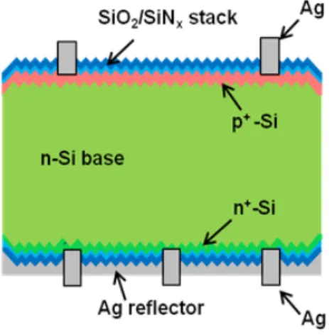
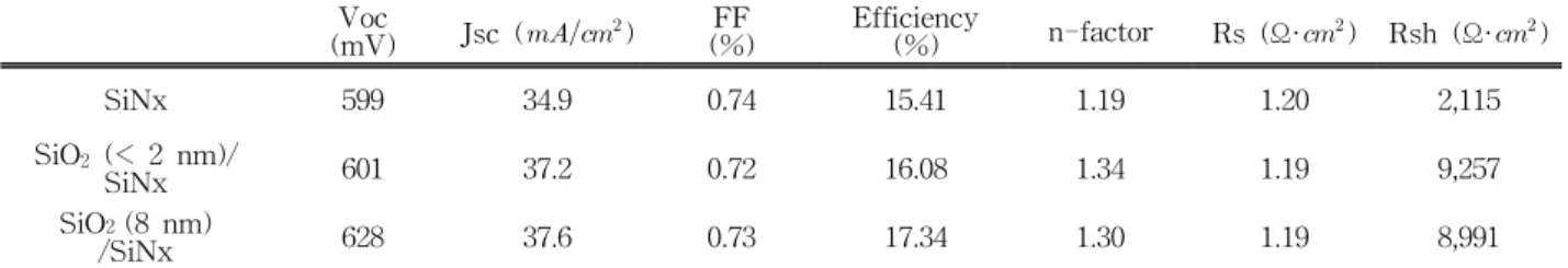
Abstract: SiO2 layer grown by rapid thermal oxidation and SiNx layer were used for passivating the surface of n-type silicon solar cell, instead of only SiNx layer generally used in p

hotovoltaic

industry.

The rapid thermal oxidation provides the reduction of processing time and avoids bulk life time degradation during the processing. Improvement of 30 mV in Voc and 2.7 mA/cm2 in Jsc was obtained by applying these two layers. This improvement led to fabrication of a large area (239 cm2) n-type solar cell with 17.34% efficiency. Internal quantum efficiency measurement indicates that the improvement comes from the front side passivation, but not the rear side, by using SiO2/SiNx stack.

Keywords: n-type solar cell, Rapid thermal oxidation

1. 서 론

N-type 실리콘의 탁월한 전기적인 특성으로 인해

a. Corresponding author; [email protected] Copyright ©2013 KIEEME. All rights reserved.

This is an Open-Access article distributed under the terms of the Creative Commons Attribution Non-Commercial License (http://creativecommons.org/licenses/by-nc/3.0) which permits unrestricted non-commercial use, distribution, and reproduction in any medium, provided the original work is properly cited.

서 최근 n-type 실리콘 기반의 태양전지의 고효율화

가 크게 주목을 받고 있다 [1-5]. 또한 n-type 실리콘

태양전지는 기존의 p-type 실리콘 태양전지에서 종종

발견되는 light-induced degradation 현상이 발견되지

않는다는 큰 장점을 가지고 있다 [6,7]. 하지만 이러

한 고효율의 n-type 태양전지를 제작함에 있어서 여

러 가지 공정 상에 문제점이 제기되고 있지만, 가장

큰 이슈는 p+ 영역의 효과적인 보호막 형성과 고효

(2)

전기전자재료학회논문지, 제26권 제1호 pp. 18-21, 2013년 1월: 류경선 등 19

Fig. 1. Schematic of n-type solar cell structure passivated by RTO SiO

2

and PECVD SiNx stack.

율 획득에 관한 것이다. 태양광 산업에서 흔히 쓰이 는 PECVD (plasma-enhanced chemical vapor deposition)을 이용한 SiNx 보호막은 n+ 영역을 보호 하는데 효과적이지만, p+ 영역에는 부정적인 효과를 초래한다 [8]. 따라서, 고효율의 태양전지를 제작하기 위해서는, p+ 영역에 적합한 표면 보호막을 사용하는 것이 아주 중요하다. 따라서 본 논문에서는 효과적인 p+ 영역의 표면 보호를 위해서 RTO (rapid thermal oxidation) 방식으로 형성된 SiO

2

보호막을 적용시켜 소 자를 제작하였다. 이 방식은 기존의 furnace oxidation 방식보다 공정 시간이 매우 짧고, 공정 중에 발생할 수 있는 bulk lifetime degradation 유발을 미리 방지할 수 있는 장점이 있다 [9]. RTO SiO

2

보호막을 이용한 239 cm

2

의 크기 (가로, 세로의 길이는 각각 15.24 cm)를 가지는 대면적 고효율 n-type 실리콘 태양전 지를 제작하고, IQE (internal quantum efficiency) 측 정을 통해 n-type 태양전지에 미치는 RTO SiO

2

의 전기적인 특성을 분석하였다.

2. 실험 방법

그림 1은 이번 연구에서 제작된 239 cm

2

의 n-type 실리콘 태양전지의 구조를 나타낸다. 태양전지 제작 에는 5 Ω·cm 저항 그리고 190 μm 두께의 n-type Cz 웨이퍼를 사용하였다. 웨이퍼 양쪽 표면은 피라미드 형태로 텍스처링 (texturing)을 실시하였고, 표준 습식

세정 공정을 수행하였다. 후면은 phosphorus dopant 를 이용해서 임플란트 공정을 실시하였고, 전면은 inkjet-printing 방식을 이용해 boron source을 도포하 였다. 그리고 950℃ 온도에서 1시간 동안의 열처리 과정을 거쳤다. 열처리 과정 이후, 45 Ω/sq boron emitter와 50 Ω/sq phosphorus BSF (back surface field)가 형성되었다. 표면 보호막으로는 SiO

2

가 사용 되었고, RTO를 통해 웨이퍼 양쪽 면으로 생성하였다 [9]. 또한 SiO

2

보호막 위에 PECVD 공정을 이용하여 70 nm의 두께를 가지는 SiNx 반사 방지막 (anti-reflection coating) 증착하였고, 컨택 형성을 위 해서 screen-printing 작업을 수행하였다. 전면은 그 리드 패턴 (gird-pattern)으로 프린팅되었고, 후면은 반복적인 dot 형태의 패턴으로 작업하였다. 여기서 전 면 프린팅은 silver와 aluminum이 혼합된 paste가 사 용되었고, 후면 프린팅은 silver paste만을 이용하여 제작하였다. Screen-printing 이후, 샘플들은 700℃

이상의 온도에서 belt furnace에서 firing 단계를 거치 셔 소자 및 전극 안정화 작업을 진행하였다. 마지막 으로, 후면의 silver dot들을 연결하기 위해서 silver reflector를 후면에 페인팅을 하고 belt dryer 안에서 400℃의 온도에서 건조 과정을 실시하여 최종적인 태 양전지 소자를 완성하였다.

3. 결과 및 고찰

표 1은 n-type 태양전지의 전기적인 특성인 I-V 결과들을 나타낸다. 일반적으로 p-type 태양전지에서 n+가 도핑된 부분에는 PECVD SiNx가 표면 방지막으로 효과적으로 사용되었다. 하지만 SiNx는 n-type 태양전지의 p+ 도핑된 지역의 표면 방지막으로서는 적합하지 않다.

표 1에서 보듯이 SiNx를 사용하였을 경우, n-type 태양전지의 전기적인 성능은 매우 낮아진다. 실제로 Voc는 599 mv, Jsc는 34.9 mA/cm

2

, 그리고 효율은 15.41%로 측정되었다. P+ 표면과 SiNx 표면 방지막 사이에 defects들이 생기고, 그것으로 인해서 전자-정공의 재결합의 장소 역할을 하기 때문이다 [8].

본 연구에서는 표면의 결점들을 보완하기 위해 표면 방지막으로 SiO

2

가 사용하였다. 일반적으로 furnace에서 형성되는 SiO

2

의 박막 제조 공정 시간은 매우 길다.

그리고 이러한 긴 공정 시간으로 인해서 실리콘 bulk

lifetime 에 전하 포획 등의 부정적인 영향을 준다.

(3)

20 J. KIEEME, Vol. 26, No. 1, pp. 18-21, January 2013: K. Ryu et al.

Table 1. I-V characteristics of n-type solar cells with different passivation.

Voc

(mV) Jsc (   

) FF

(%) Efficiency

(%) n-factor Rs (Ω· 

) Rsh (Ω· 

)

SiNx 599 34.9 0.74 15.41 1.19 1.20 2,115

SiO

2

(< 2 nm)/

SiNx 601 37.2 0.72 16.08 1.34 1.19 9,257

SiO

2

(8 nm)

/SiNx 628 37.6 0.73 17.34 1.30 1.19 8,991

따라서 본 논문에서는 대면적 n-type 실리콘 태양전지의 SiO

2

표면 방지막을 제작하기 위해 RTO를 사용하였다. 900℃에서 2분 간의 RTO 공정을 통해 형성된 얇은 SiO

2

보호막과 PECVD를 적용한 SiNx 방지막을 함께 적용했을 때의 태양전지의 전기적인 특성은 SiNx만을 사용했을 경우보다 성능이 향상됨을 알 수 있었다. Voc는 601 mV, Jsc는 37.2 mA/cm

2

, 효율은 16.08%로 측정되었다. 그러나 성능 향상의 정도는 매우 작은데, 이것은 SiO

2

보호막이 너무 얇아서 (< 2 nm) 충분한 보호막 효과를 얻을 수 없었기 때문이다. 따라서 고효율의 태양전지를 제작하기 위해 900℃에서 10분 간의 RTO를 통해 8 nm의 두께를 가지는 SiO

2

보호막과 PECVD SiNx 방지막을 증착하였다. N-type 태양전지의 성능은 표 1의 결과에서처럼 매우 향상되었다. Voc는 628 mV, Jsc는 37.6 mA/cm

2

, 그리고 효율은 17.34%가 측정되어 N-type 태양전지의 성능이 기존의 PECVD SiNx 방지막을 가지는 소자보다 크게 향상되었다. 이러한 성능 향상은 RTO SiO

2

가 효과적으로 p+ 표면을 보호한다는 것을 충분히 입증하였다. 또한 RTO SiO

2

보호막은 전면과 후면에 동일하게 형성되었기 때문에, 이러한 성능 향상이 어디에서 오는지 정확하게 물리학적으로 분석하기 위해서 IQE 측정 실험을 추가적으로 하였다.

그림 2는 SiNx과 RTO SiO

2

/SiNx 표면 보호막이 사용된 n-type 태양전지의 IQE 결과를 보여준다.

그림 2에서 보는 것처럼, 단파장 영역에서의 (350 nm ∼ 650 nm) IQE 결과가 보호막의 종류에 따라 다르다는 것을 알 수 있다. RTO 기반의 SiO

2

/SiNx 경우, 단파장에서의 IQE가 더 높은 반응을 보인다.

하지만 장파장의 영역에서는 (900 nm ∼ 1,200 nm), 두 셀의 IQE는 서로 동일한 결과를 나타내었다.

Fig. 2. IQE comparison of n-type solar cells passivated SiO

2

/SiNx and only SiNx.

이것은 RTO SiO

2

/SiNx 표면 방지막은 후면 (n+

영역)이 아닌 전면 (p+ 영역)에서 매우 효과적으로 작용한다는 것을 나타내었다. 따라서 이러한 효과적인 표면 방지막을 사용함으로써, 전면으로부터 향상된 Voc와 Jsc를 얻을 수 있었다.

4. 결 론

P+ 영역 표면 방지를 위해 SiO

2

/SiNx 보호막을 이용하여 대면적 n-type 실리콘 태양전지를 제작하였다.

8 nm의 두께를 가지는 RTO SiO

2

보호막은 매우

효과적으로 p+ 영역을 보호하여 17.34%의 효율을

가지는 n-type 태양전지를 제안하였다. 또한, IQE

측정을 통해 RTO SiO

2

보호막은 p+ 영역을

보호하는데 효과적인 역할을 한다는 것을 확인하였고,

향후 대면적 에너지 하베스팅 전자소자를 만들기

위한 핵심 기술로 사용할 수 있다고 판단된다.

(4)

전기전자재료학회논문지, 제26권 제1호 pp. 18-21, 2013년 1월: 류경선 등 21

감사의 글

이 논문은 2011년도 충북대학교 학술연구지원사업의 연구비 지원에 의하여 연구되었음 (This work was supported by the research grant of the Chungbuk National University in 2011).

REFERENCES

[1] S. W. Glunz, S. Rein, J. Y. Lee, and W. Warta, J.

Appl. Phys., 90, 2397 (2001).

[2] D. Macdonald and L. J. Geerligs, Appl. Phys. Lett., 85, 4061 (2004).

[3] J. E. Cotter, J. H. Guo, P. J. Cousins, M. D. Abbott,

F. W. Chen, and K. C. Fisher, IEEE Trans. Elec.

Dev., 53, 1893 (2006).

[4] C. L. Andre, J. A. Carlin, J. J. Boeckl, D. M. Wilt, M.

A. Smith, A. J. Pitera, M. L. Lee, and S. A. Ringel, IEEE Trans. Elec. Dev., 52, 1055 (2005).

[5] Z. Wu, T. Song, Tao, Y. Jin, and B. Sun, Appl. Phys.

Lett., 99, 143306 (2011).

[6] J. Schmidt, A. G. Aberle, and R. Hezel, Presented at the 26th IEEE PVSC (Anaheim, 1997)

[7] H. Jiang, S. Seyedmohammadi, A. Shaikh, and E.

Graddy, 37th IEEE Photovoltaic Specialists Conference (U.S.A., 2011) p. 001458.

[8] J. Schmidt, F. M. Schuurmans, W. C. Sinke, S. W.

Glunz, and A. G. Aberle, Appl. Phys. Lett., 71, 252 (1997).

[9] R. Singh, J. Appl. Phys., 63, R59 (1988).

수치

Fig.  1.  Schematic  of  n-type  solar  cell  structure  passivated  by  RTO  SiO 2   and  PECVD  SiNx  stack.
Table  1.  I-V  characteristics  of  n-type  solar  cells  with  different  passivation.

참조

관련 문서

The study was made to reduce the weight of the body by using Friction Stir Welding (FSW), which is a solid joining process of low heat input type in order to solve

This study was conducted to investigate the storage period and optimal temperature of seed potato which were based on technique of dormancy prolonging by

This is because that the thermal conductivity and solar weighted absorption fraction of MWCNT/Fe 3 O 4 hybrid nanofluid is lower than those of MWCNT

Therefore, in this paper, the solar array of HST is modeled as a simple model with beams and membranes, and the phenomenon of thermal induced vibration is verified and

은 다른 버전이 쏟아졌다 원곡의 보컬 부분만 따와서는 여기에 새로운 반주를 더. 하여 완전히 다른 분위기의 매력적인 곡들이 숱하게 만들어졌던 것이다.

(Note 3) This value is displayed by timer events set in the event and by the operation type of the external switch input set to the timer start setting. As long as

While a chemical reac- tion takes place between different synthons and typically yields a unique molecule after each synthetic step, layer-by-layer deposition involves the

The builtin package defines error as an interface with a single Error() method that returns an error message as a string.. We’ll see