DOI: http://dx.doi.org/10.4313/JKEM.2013.26.1.13
LED 구동 IC를 위한 레벨 시프터 방식의 전하펌프 회로 설계
박원경1, 박용수2, 송한정1,a
1 인제대학교 나노시스템공학과
2 충청대학교 전기전자학부
Design of a Charge Pump Circuit Using Level Shifter for LED Driver IC
Won-Kyeong Park
1, Yong-Su Park
2, and Han-Jung Song
1,a1 Department of Nano Engineering, Inje University, Gimhae 621-749, Korea
2 Department of Electronics, Chungcheong University, Cheongju 363-792, Korea
(Received September 27, 2012; Revised November 29, 2012; Accepted December 3, 2012)
Abstract: In this paper, we designed a charge pump circuit using level shifter for LED driver IC. The designed circuit makes the 15 V output voltage from the 5 V input in condition of 50 kHz switching frequency. The prototype chip which include the proposed charge pump circuit and its several internal sub-blocks such as oscillator, level shifter was fabricated using a 0.35 um 20 V BCD process technology.
The size of the fabricated prototype chip is 2,350 um × 2,350 um. We examined performances of the fabricated chip and compared its measured results with SPICE simulation data.
Keywords: CMOS, Charge pump, LED display, Level shifter, SPICE simulation, Chip fabrication
1. 서 론1)
액정 디스플레이(LCD)는 최근 각종 전자제품의 디스 플레이를 위한 핵심부품으로 광범위하게 사용되고 평판 디스플레이 중 하나로, 매년 수요가 급성장하고 있다.
LCD는 별도의 자체발광 소자가 아니기 때문에 별도의 광원을 필요로 한다 [1]. 그 중 가장 대표적인 광원으로 는 냉음극 형광램프 (CCFL)와 발광 다이오드 (LED)가
a. Corresponding author; [email protected]
Copyright ©2013 KIEEME. All rights reserved.This is an Open-Access article distributed under the terms of the Creative Commons Attribution Non-Commercial License (http://creativecommons.org/licenses/by-nc/3.0) which permits unrestricted non-commercial use, distribution, and reproduction in any medium, provided the original work is properly cited.
있다. CCFL은 LCD의 화면이 커질수록 가격이 비싸지는 단점이 있으며, 또한 환경문제가 점점 사회의 주요한 이 슈로 대두되면서 독성이 있는 수은을 포함하는 CCFL의 사용을 점진적으로 금지하려는 움직임들이 세계 주요 각 국에서 일어나고 있다. 이에 따라, 긴 동작수명, 광범위 한 동작 온도, 단순한 드라이버 회로, 안전한 저전압 동 작 등의 장점을 가진 LED가 점차 CCFL 백라이트를 대 체하고 있다. LED는 전기신호가 인가되면 빛을 발산하 는 화합물 반도체의 일종으로 발광 다이오드라고 하며 화합물 반도체의 조성비를 조절함으로써 다양한 색상구 현이 가능하다. 이처럼 LED 활용도가 증가하면서 더불 어 LED 구동회로의 중요성도 증가하고 있다. 전하펌프 (charge pump) 방식을 이용하여 LED 구동회로를 구성 하면 빠른 안정화 시간, 높은 효율, 낮은 소비전력, 출력 전압의 낮은 ripple과 EMI 특성을 만족시킬 수 있다. 최
발표되고 있으나 효율과 전력 소모 개선 등 역구의 여지 가 많은 것이 사실이다 [2-4]. 본 논문에서는 가변전압 방식의 레벨시프터를 사용하여 DC-DC 변환기에 필요한 새로운 전하펌프 회로를 구현한다. II장에서 본 논문에서 제안하는 전하펌프 회로의 구성을 언급한다. III장에서 제안하는 회로에 대한 SPICE 모의실험, IV장에서, 칩제 작 및 제작된 칩의 특성 결과를 살펴보고 마지막으로 V 장에서 결론은 내린다.
2. 실험 방법
2.1 제안하는 레벨시프터 방식의 전하펌프
그림 2에 제안하는 LED 구동회로용 전하펌프 블록 도를 나타내었다. 일반적인 구조에 가변전압 레벨시 프터를 추가하여 가장 높은 전압레벨인 출력전압을 이용하여 전하펌프의 스위치 트랜지스터의 게이트를 구동하는 전압레벨을 만들어 낸다.
Fig. 1. Block diagram of the proposed charge pump for LED driver.
제안하는 회로는 기존의 NMOS 구성회로의 NMOS를 PMOS로 대체함으로써, 부가적인 공정을 감소시켰고, 출력전압을 이용하여 각 단마다 크고 일 정한 VGS 전압을 인가하므로 전체적인 RON값을 감소 시켰다. 또한 스위치 트랜지스터 구동 시 소모되는 스위칭 손실을 최소화시켜 전력 효율을 증가시켰다.
그림 3에 기존의 딕슨 방식의 전하펌프 회로와 제 안하는 전하펌프 회로를 나타내었다 [5-7].
Fig. 2. Comparison between Dickson and proposed charge pump. (a) Dickson charge pump, (b) proposed charge pump using a variable boltage level shifter.
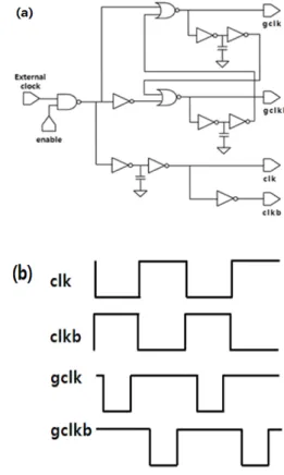
Fig. 3. Clock generator and timing diagram for charge
pump. (a) clock generator, (b) timing diagram.
Fig. 4. Level shifter using the variable voltage.
그림 4는 전하펌프의 스위치 트랜지스터를 구동하 는 클럭 발생회로와 그 타이밍도이다. 스위치 트랜지 스터의 턴 온 시 전압레벨은 가변전압 레벨 시프터 (level shifter)를 통하여 조절되고, 턴 오프 시 전압레 벨을 제어하기 위해 GP1, GP2의 트랜지스터를 펌프 단과 스위치 트랜지스터의 게이트 사이에 연결하였다 [1]. 각 단이 턴 오프 상태일 때, VG1, VG2 전압은 다 르지만 턴 온될 때, VG1, VG2의 전압은 같게 된다.
3. 결과 및 고찰
3.1 SPICE 시뮬레이션 결과 및 레이아웃
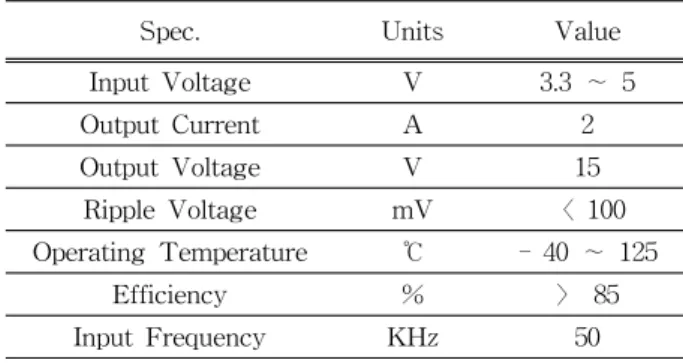
표 1에, 본 논문에서 설계하고자 하는 전하펌프의 설계 명세서를 나타내었다.
Table 1. Specification of the proposed charge pump.
Spec. Units Value
Input Voltage V 3.3 ∼ 5
Output Current A 2
Output Voltage V 15
Ripple Voltage mV 〈 100
Operating Temperature ℃ - 40 ∼ 125
Efficiency % 〉 85
Input Frequency KHz 50
Fig. 5. Simulated results of the timing clocks.
Fig. 6. Simulated output result of the charge pump.
Fig. 7. Prototype chip layout for the proposed charge pump.
그림 6에 클럭 발생회로 타이밍도를 나타내었다.
제안하는 회로는 주파수 50 kHz에서 동작하며, 효율 은 약 85%이다.
그림 5는 제안하는 LED 구동용 전하펌프의 출력전 압을 나타내고 있으며, 5 V 인가 시 입력전압의 3배
음을 확인할 수 있다. 제안하는 회로는 0.35 um BCD 공정으로 설계되었으며, 테스트를 위한 주요 블록 및 전체 회로를 포함한 크기는 2,350 um × 2,350 um로 레이아웃하였다.
3.2 칩 제작 및 측정 분석
본 논문에서 제안한, 레벨시프터 방식의 전하펌프 회로는 회로 레이아웃을 거쳐, 최종적으로 0.35 um BCD 공정에 의해 제작되었다.
Fig. 8. (a) Photomicrograph of the fabricated chip (b) PCB board of the packaged chip.
제작된 칩은 80 pin LQFP 형태로 패키징을 하였 고, 패키징된 프로토 타입 칩은 PCB 보드를 구성하 여 오실레이터, 레벨시프터 등 개별 TEST 블록과 전 체회로를 측정하였다.
그림 8(a)와 (b)는 각각 칩의 현미경 사진과 칩 장 착 PCB 보드 사진이다. 제작된 칩 측정 결과 오실레 이터 같은 경우 결과 값이 제대로 나오지 않았는데, 내부에 쇼트가 났기 때문인 것으로 추정된다.
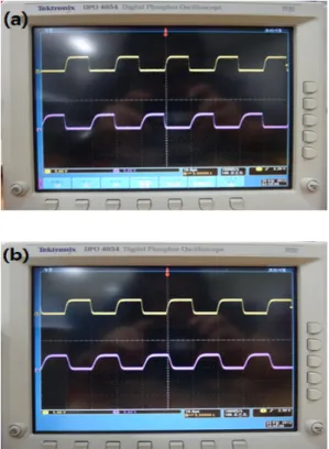
Fig. 9. Measured output pulse of the level shifter.
Fig. 10. Measured output of the timing clocks. (a) output of gclk, gclkb, (b) output of clk, clkb.
그 외 드라이버, 레벨 시프터, 클럭 발생기는 그림 에서 나타난 것처럼 설계했던 것과 같이 결과 값이 나왔지만, 시간이 지나면 칩이 타버리는 현상이 나타 났다. 그 이유는 전류가 설계했던 것보다 높게 흘렀 는데, 메탈 폭이 좁아 전류량을 견디지 못하는, 일렉 트로 마이그레이션 (electro migration) 현상이 나타난 것으로 추정된다.
4. 결 론
제안하는 회로는 0.35 um BCD 공정을 사용하여 설계, 레이아웃되었다. 설계 결과 입력전압 5 V가 3 배 승압된 15 V의 출력 전압을 얻을 수 있었다. 제작 된 prototype 칩에 대한 측정을 실시하였고, 개별 회 로 테스트 결과 오실레이터를 제외한 드라이버, 레벨 시프터 등 각종 sub-block의 정상적인 동작을 대부분 확인하였다. 오실레이터의 오동작으로, 전체 전하펌프 회로의 정상적인 동작은 이루어지지 않았다. 향후, 이 러한 면을 고려하며, 좀 더 개선된 회로 설계가 가능 하리라 사료된다.
감사의 글
This work was sponsored by ETRI SW-SoC R&BD Center, Human Resource Development Project.
REFERENCES