An Experimental Study on Wafer Demounting by Water Jet in a Waxless Silicon Wafer Mounting System
Kyoungjin Kim, Ho Sang Kwak
†and Kyoungseok Park
†
School of Mechanical Engineering, Kumoh National Institute of Technology
ABSTRACT
In the silicon wafer polishing process, the mounting stage of silicon wafer on the ceramic carrier block has been using the polishing template which utilizes the porous surface instead of traditional wax mounting method. Here in this article, the experimental study is carried out in order to study the wafer demounting by water jet and the effects of operating conditions such as the water jet flowrate and the number of water jet nozzles on the wafer demounting time. It is found that the measured wafer demounting time is inversely proportional to the water flowrate per nozzle, regardless of number of nozzles used; implying that the stagnation pressure by the water jet impingement is the dominant key factor.
Additionally, by using the transparent disk instead of wafer, the air bubble formation and growth is observed under the disk, making the passage of water flow, and subsequently demounting the wafer from the porous pad.
Key Words : Silicon Wafer, Waxless Wafer Mounting, Wafer Demounting, Water Jet
1. Introduction
Silicon wafers have been used as a substrate for a vast majority of microelectronics semiconductor devices and they must be very flat in order to have circuits printed on them by lithographic processes.
Wafer flatness represents the one of most important aspects in wafer quality and directly impacts device line-width, process latitude, production yield, and throughput [1,2]. Wafer surface polishing is one of many important processes in manufacturing silicon wafers. After silicon ingot is sliced into the thin wafers, the wafers go through the several stages of surface polishing, where the wafers achieve the ultra high flatness on their surfaces. Before and after entering those polishing stages, the wafers need to be mounted on a carrier block and then demounted from the block, respectively.
One of the popular methods for mounting the wafer on the carrier block is so called wax mounting which uses a thin wax layer between the wafer and the
carrier block. The wax in the form of highly viscous liquid is applied on the surface of ceramic carrier block usually by a spin coater and the wafer is brought into the contact with the wax coated carrier block [3]. Wax mounting has been wildly used, especially since the global flatness of wafer surface can be achieved. However, wax mounting is known to possess several disadvantages. First, the mounting process becomes rather complicated by requiring the heating of wax layer right after wafer is mounted and the dissolving of wax layer by solvent when unmounted.
Also, the wax mounting requires a relatively thorough cleaning of the wax coated surface of both the wafer and the carrier block. Additionally, the use of solvent for demounting has cost and environmental implications [4].
In terms of wafer polishing quality, wax mounting has a great success in having very high global flatness, but shows weakness in having good site flatness (or local flatness). Although the global flatness is still important, the site flatness has become more critical in today’s microelectronics technologies, since the miniaturization of semiconductor devices are ever progressing due to technological advances.
†
E-mail : hskwak@kumoh.ac.kr
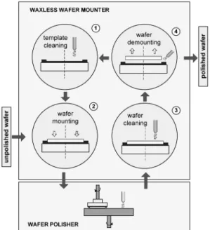
In response to those shortcomings in wax mounting, silicon wafer manufacturers turn to waxless mounting technique, which eliminates the use of mounting wax and instead uses porous template. Fig. 1 shows the typical process flow for the silicon wafer mounting on a carrier block before and after wafers going through single side wafer polishing, and it is consisted of wafer mounting on the wetted template, wafer demounting from the template, and cleaning of wafer and template surfaces. Compared to conventional wax mounting, waxless mounting provides more environ- mentally friendly and easier cleaning, while a better site flatness can be accomplished when the mounted wafers are polished.
Mounting the wafers on the template is convenient, however, demounting the wafers from the template is relatively difficult task and the wafers can be damaged if mishandled. Therefore, it could be a potential bottleneck in the wafer preparation stages for surface polishing. In this article, demounting of silicon wafers from the porous template by DI water jet is inves- tigated experimentally in an effort to find the operating conditions for a reliable demounting without risking the surface quality of the handled wafers.
2. Experimental
A porous template used in waxless wafer mounting is consisted of three parts: porous mounting pad, retainer ring, and the mounting adhesive on the back, as illustrated in Fig. 2. Wafer resides on the porous mounting pad which is attached to a carrier block.
Porous mounting pad provides secure wafer adhesion through a suction force in its sponge-like structure once the wafer is pressed onto the wetted pad surface.
As shown in the microscopic photograph of Fig. 3, the pore size of mounting pad ranges from 50 to 100 mm. The porosity of the mounting pad is approximately 40 percent and its thickness is approximately 0.64 mm when its surface is dry and not pressed.
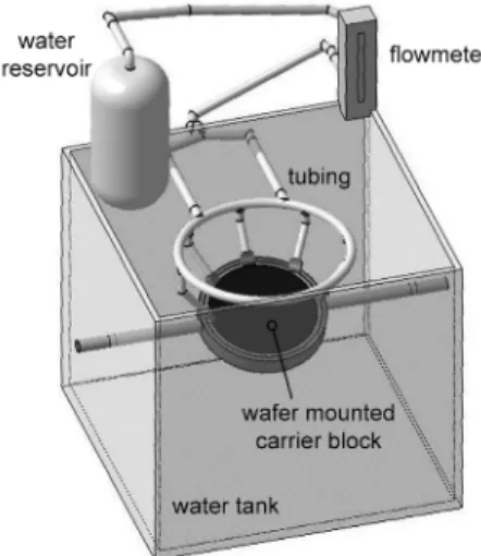
The photograph in Fig. 4 and the illustration in Fig.
5 show the experimental setup for wafer demounting, while Fig. 6 illustrates a detailed frontal view of the Fig. 1. Schematic illustration of waxless wafer mounting
in silicon wafer polishing station.
Fig. 2. Cutaway view of the wafer mounted carrier block using a porous template (not to scale).
Fig. 3. Microscopic morphology of porous surface on the
wafer mounting template.
previously mentioned carrier block with the silicon wafer mounted on the template accompanied by a water jet system for wafer demounting. Water is supplied from the water reservoir and enters to the tubing system. The volumetric flowrate of water is measured by a float displacement type flowmeter (Unicell LF301), which is capable of handling up to 15 liter/min (lpm) of water flow. There are five water nozzles in the water jet system, as the locations of the nozzles are shown in Fig. 6. With respect to the center of wafer, five nozzles cover 180 degrees of upper side of the wafer and 45 degrees apart between them, while every nozzle is in the same distance from the wafer. Each water nozzle has sixteen holes which diameters are 1 mm. Those holes are placed in line and the spacing between neighboring holes is 2 mm.
In the present experiments, each individual nozzle is detachable from the tubing and the following four combinations of the nozzle arrangement are tested:
single nozzle case (nozzle 1); two nozzle case (nozzles 2 and 3); three nozzle case (nozzles 1, 2, and 3); five nozzle case (nozzles 1, 2, 3, 4, and 5).
Inclination of the wafer mounted carrier block can be adjusted to a certain degree, so the wafer slides down after it is demounted by water jet. Note that, in the actual automated manufacturing process, the demounted wafers can slide into the wafer cassette storage unit. Silicon wafers used in the experiments are 200 mm (8 inches) in diameter and 0.7 mm in thickness. They are already polished commercial quality wafers and obtained from the silicon wafer mass manufacturer. Dimensions of the circular carrier block are 230 mm in diameter and 22 mm thickness.
In this experimental research, the effects of water jet strength and the nozzle combinations on the wafer demounting are investigated. Also, the understanding of wafer demounting mechanism from the porous pad is one of the objectives in this study.
3. Results and Discussion
In each wafer demounting test, the secure wafer mounting on the porous template is prepared by applying a constant force of 60 kgf for 30 seconds evenly on the wafer that is already placed on the Fig. 4. Experimental setup for waxless wafer mounting
with water jet.
Fig. 5. Three dimensional view of the experimental setup for waxless wafer mounting.
Fig. 6. Detailed frontal view of wafer mounted carrier
block with the water nozzle arrangement.
wetted surface of porous mounting pad. Inclination angle of the wafer mounted carrier block is set to be 20 degrees in each test. Also, water jet from the nozzles is adjusted to aim the outer edge of the wafer with jet direction of 45 degrees. The distance from the nozzle to the edge of the wafer is approximately 3 cm.
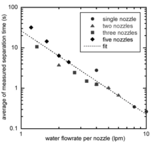
As previously mentioned, total four cases of nozzle combinations are tested for the water flowrate varying from 2 to 12 lpm. Time for wafer demounting is measured ten times in each test and the averaged results are shown in Fig. 7. At a given flowrate, the cases with less number of nozzles are found to result in a shorter demounting time. Those experimental results in Fig. 7 are plotted against the flowrate per nozzle in Fig. 8. In a log-log scale, the measured data
of wafer demounting time from all the cases of nozzle combination fall into the straight fitting line, although the data scattering becomes larger at lower water flowrates. This power fit is found to be
T = 27.6( /N)
-2.04where T, , and N are the wafer demounting time (in seconds), total water flowrate (in lpm), the number of nozzle used in the test, respectively.
The water flowrate per nozzle ( /N) is directly proportional to the water jet velocity. When the water jet is impinged onto the wafer, we expect the stagnation pressure on the jet impact point, which is proportional to the square of water jet velocity. It is possibly the stagnation pressure created by water jet and applied into the gap between the wafer and the mounting pad that is the key factor to decide the wafer demounting time. This is consistent with the power of -2.04 found in the data fitting. Thus, the strength of the water jet in an individual nozzle, which is represented by the stagnation pressure, is the dominant factor in overcoming the suction force and demounting the wafer from the porous template pad, while the total amount of the water jet flowrate or the number of nozzle show insignificant effects.
In other words, the integrated quantity from all the water jet nozzles such as total flowrate or total pressure acting on a whole wafer is not important.
Instead, even if there are multiple water jet nozzles working together, it would be the one particular water jet nozzle that gives the enough disturbances to very local area in order to free the mounted wafer from the suction force of porous mounting pad.
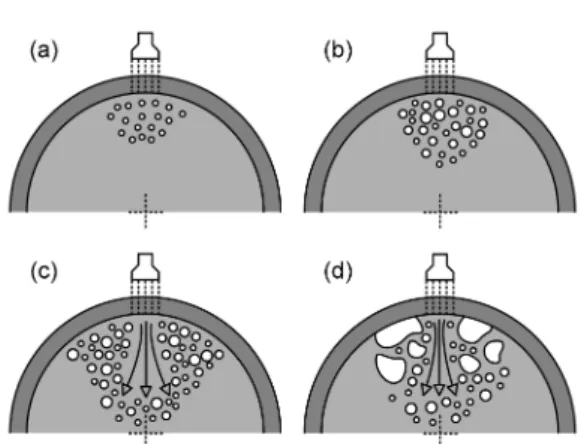
In order to visually investigate and understand the demounting mechanism of wafer from the porous mounting pad, the silicon wafer is replaced by the transparent polycarbonate disk of the same size on the carrier block and is subjected to the water jet system.
During this test, only one nozzle is used to inspect the demounting more clearly. The air bubble formation and growth is observed underneath the transparent disk. It is quite difficult to visualize those phenomena due to the reflective nature of water flowing surface.
Instead, this observation is illustrated in Fig. 9, showing the transitory formation and growth of air bubbles
Q · Q ·
Q ·
Fig. 7. Effect of nozzle combination and water flowrate on wafer demounting time.
Fig. 8. Effect of water flowrate per nozzle on wafer
demounting time.
when the water jet is impinged into the wafer edge.
At first, there is no formation of air bubbles observed for a while after the initiation of water jet.
However, as shown in Fig. 9(a), a number of small air bubbles start to appear under the disk around the location of water jet impingement several seconds before wafer demounting. A possible reason for this bubble formation might be that the air is pushed into the porous pad when the water jet impacts the narrow gap between the disk and the retainer ring of template and then small air bubbles form after air entrained by water jet appears on the back side of disk through fine porous structure of the pad. Those air bubbles begin to grow into the larger bubbles in a short time period as shown in Fig. 9(b). Formation of those larger air bubbles seems to make enough passage for water jet to penetrate between the surfaces of mounted disk and the porous pad. As depicted in Fig. 9(c), the water flow can be observed and it pushes away the air bubbles into all directions. Introduction of water flow under the disk makes the gap between the disk and the porous pad even wider and the air bubbles collapse into larger ones of irregular shape, shown in Fig. 9(d). When those irregular shaped air bubbles become sufficiently large, the disk becomes demounted and slipped down over the inclined template surface.
4. Conclusions
This article addresses the research and development
of wafer demounting technique using the water jet impingement for a waxless wafer mounting system.
An experimental setup is built to study the mechanism of wafer demounting by water jet and the effectiveness of water jet in wafer demounting. Experimental results show that the water jet strength such as stagnation pressure in an individual water nozzle is more important than the flowrate itself. Also, the air bubbles are observed underneath the wafer around the area of water jet impingement, starting to grow and merge and making water passage, which results in immediate wafer demounting from the porous template surface.
Acknowledgement
This research was financially supported by the 16th Industry-Academic Cooperation R&D Program from the Gyeongbuk Provincial Government and Small and Medium Business Administration (SMBA).
References
1. Pei, Z. J., Fisher, G. R., and Liu, J., “Grinding of Sil- icon Wafers: A View from Historical Perspectives,”
International Journal of Machine Tools and Manufac- ture, Vol. 48, pp. 1297-1307, 2008.
2. Sun, W., Pei, Z. J., Fisher, and G. R., “Fine Grinding of Silicon Wafers: Effects of Chuck Shape on Grind- ing Marks,” International Journal of Machine Tools and Manufacture, Vol. 45, pp. 673-686, 2005.
3. Noh, Y. M., Im, I. T., and Kim, K. S., “A Numerical Study on Combined Solution and Evaporation during Spin Coating,” Journal of The Korean Society of Semiconductor & Display Equipment Technology, Vol. 2, pp. 25-29, 2003.
4. Combe, S., Cullen, J., and O’Keefe, M., “Reversible Wafer Bonding: Challenges in Ramping up 150 mm GaAs Wafer Production to Meet Growing Demands,”
CS MANTECH Conference, Vancouver, British Colum- bia, Canada, 2006.
접수일: 2009년 5월 21일, 심사일: 2009년 6월 5일 게재확정일: 2009년 6월 15일