반도체디스플레이기술학회지 제17권 제3호(2018년 9월)
Journal of the Semiconductor & Display Technology, Vol. 17, No. 3. September 2018.
Role of a PVA layer During lithography of SnS 2 thin Films Grown by Atomic layer Deposition
Giyul Ham
*, Seokyoon Shin
*, Juhyun Lee
*, Namgue Lee
**and Hyeongtag Jeon
*†*†
Department of Materials Science and Engineering, Hanyang University, Seoul, 133-791, Korea
**
Department of Nanoscale Semiconductor Engineering, Hanyang University, Seoul, 133-791, Korea
ABSTRACT
Two-dimensional (2D) materials have been studied extensively due to their excellent physical, chemical, and electrical properties. Among them, we report the material and device characteristics of tin disulfide (SnS 2 ). To apply SnS 2 as a channel layer in a transistor, SnS 2 channels were formed by a stripping method and a transfer method. The limitation of this method is that it is difficult to produce uniform device characteristics over a large area. Therefore, we directly deposited SnS 2 by atomic layer deposition (ALD) and then performed lithography. This method was able to produce devices with repeatable characteristics over a large area. However, the SnS 2 film was damaged by the acetone used as a photoresist (PR) developer during the lithography process, with the electrical properties of mobility of 2.6x10 -4 cm 2 /Vs, S.S. of 58.1 V/decade, and on/off current ratio of 1.8x10 2 . These results are not suitable for advanced electronic devices. In this study, we analyzed the effect of acetone on SnS 2 and studied the device process to prevent such damage. Using polyvinyl alcohol (PVA) as a passivation layer during the lithography process, the electrical characteristics of the SnS 2 transistor had 2.11x10 -3 cm 2 /Vs of mobility, 11.3 V/decade of S.S, and 2.5x10 3 of the on/off current ratio, which were 10x improvements to the SnS 2 transistor fabricated by the conventional method.
Key Words: Tin disulfide(SnS 2 ), Atomic layer deposition (ALD), lithography, polyvinyl alcohol (PVA)
1. Introduction
1
Two-dimensional (2D) materials typically have very strong covalent bonding forces between atoms in a layer and weak bonds between stacked layers. Because of this structural feature, 2D materials have unique mechanical/chemical/electrical/optical properties that are not observed in bulk form. 1 Therefore, studies on 2D materials and their applications have increased exponentially. 2,3 In 2004, graphene, the result of opening 2D carbon materials, was demonstrated to have promising potential in future electronic devices because of the thin critical dimension, excellent flexibility, and a high electron mobility. 1 Despite these excellent properties, graphene has no bandgap and thus has a material limit in which the on/off current ratio is poor as a channel of a transistor device. 4-6 In order to solve these problems, recent experimental studies show various results of others 2D materials that have suitable bandgaps and a layered structure similar to graphene. 7,8 In particular,
†
E-mail: [email protected]
transition metal dichalcogenides (TMDCs, MX 2 ) have attracted many researchers because they have high carrier mobility. 9 M is a transition metal element of Groups 4 to 6, and X is a chalcogen element of Group 16 (S, Se, and Te). 9,10 Among TMDCs, 2D MoS 2 has high potential as a channel material for next generation high performance, low power devices because it has high carrier mobility and an on/off current ratio with a bandgap of 1.8-1.9 eV. 7 With excellent electrical properties, earth- abundant materials are essential because of their competitive price for low manufacturing cost.
As a result of searching for 2D materials consisting of earth-abundant
elements, tin disulfide (SnS 2 ) is promising with Sn and S atoms that are
more abundant than Mo and W. 11,12 SnS 2 is a semiconductor that has a
bandgap of 2.1-2.4 eV with n-type electrical property. 11 Moreover, SnS 2
is a layered material with a hexagonal structure and consists of S-Sn-S
tri-atomic planar molecular arrangements with weak van der Waals
bonding between layers. 12 SnS 2 is being studied for application to a wide
range of uses such as field-effect transistor, 11-14 water splitting, 15 and
sensor devices 16 . In transistors, it has been reported that SnS 2 had
Giyul Ham · Seokyoon Shin · Juhyun Lee · Namgue Lee · Hyeongtag Jeon 42
mobility of 230 and 50 cm 2 /Vs and on/off current ratio of 10 7 and 10 6 . 11,12 These results were obtained using mechanical exfoliation and a transfer process. It is difficult to achieve uniform thickness over a large area using the mechanical exfoliation method. In addition, the transfer process can lead to problems of low yield for large areas and interface adhesion and instability between the device substrate and the SnS 2 channel. To solve this problem, SnS 2 should be directly deposited over a large area on a substrate and patterned for fabricating transistors. In this process, SnS 2 is affected by acetone used as a photoresist (PR) developer during the patterning process. To our knowledge, there are few studies on changes in the properties of SnS 2 by acetone as a PR developer.
In this study, we formed SnS 2 using ALD, which can be used to deposit a large area, and performed an annealing process to improve crystallinity. The results of the deposition process were previously reported by our group. 17 As a channel layer of next-generation transistors, we report the electrical properties of a device using crystalline SnS 2 formed by ALD and annealing at low temperatures. During the device fabrication process, we used a lithography process to pattern SnS 2 , and confirmed that an acetone-based PR developer damages SnS 2 films. For this reason, we investigated the changes in SnS 2 properties by the PR developer and added PVA to prevent such damage. PVA is a water- soluble polymer that can reduce the damage caused by acetone.
Through this method, the electrical properties of the SnS 2 transistor were improved by approximately 10 times.
2. Experimental
We prepared substrates for depositing SnS 2 films as follows. A substrate with 90-nm-thick, thermally-oxidized silicon dioxide (SiO 2 ) on silicon (Si) was cleaned with acetone, methanol, and deionized (DI) water using sonication for 15 min. Before the ALD process, the substrate surface was sulfurized by 99.9% hydrogen sulfide (H 2 S) gas at 150 °C.
The SnS 2 films were deposited by ALD at 150 °C. The precursor and reactant gas used in the ALD process of SnS 2 were tetrakis (dimethylamino)tin (TDMASn, [(CH 3 ) 2 N] 4 Sn) as a Sn 4+ source and H 2 S as a sulfur source, respectively. The TDMASn precursor was kept at 50 °C and transferred into the chamber using argon (Ar) bubbler gas with a flow rate of 30 sccm. The H 2 S reactant gas was injected through a metering valve. One cycle of ALD consisted of the following four steps; TDMASn precursor injection (1 s) - Ar purging (40 s) - H 2 S reactant gas injection (3 s) - Ar purging (50 s). The Ar purging gas was continuously injected into the process chamber at 200 sccm to keep the process pressure constant. A post annealing process was performed to improve the crystallinity of SnS 2 . The SnS 2 films were annealed at 300 °C using sulfur powder with a mixed gas composed of hydrogen (H 2 , 5
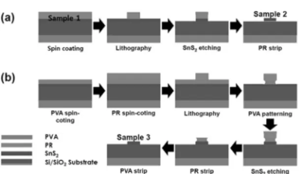
Fig. 1. Sequence of the patterning process for SnS 2 in transistor channel applications. (a) Sample 2 was directly affected by acetone, and (b) Sample 3 with PVA was not directly affected by the acetone.
sccm) and argon (Ar, 100 sccm) in a quartz tube furnace (denoted as Sample 1). The annealed SnS 2 was sonicated in acetone-based PR developer for 1 minute (denoted as Sample 2). To reduce the damage caused by acetone, PVA was applied to the surface of SnS 2 by spin coating before immersing SnS 2 in the acetone solution (denoted as Sample 3). These processes are depicted in Figure 1. The characteristics of the samples were confirmed by the following analysis methods.
The crystallinity of SnS 2 was analyzed by X-ray diffractometer (XRD) using Cu Kα radiation (λ = 1.5418 Å). The RAMAN spectra of a few-layer SnS 2 were analyzed using a MonoRA710i/ELT1000 spectrometer equipped with a silicon charge coupled device (Si-CCD).
The samples were excited with 325 nm radiation from He-Cd laser operating at a power level of 16 mW. The electrical property of SnS 2 samples was analyzed by fabricating a field effect transistor. The source/drain electrodes were metal Ti/Au (10/50 nm) deposited onto the SnS 2 channel using electron-beam evaporation. Measurements on the SnS 2 transistors were performed using a probe station (I-V measurement) at room temperature in ambient air.
3. Results and Discussion
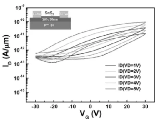
We previously published a paper on SnS 2 annealed in a H 2 /Ar (5/100 sccm) atmosphere using sulfur powder. 17 The annealed SnS 2 at 300 ° C was not re-evaporated and had the best properties, making it suitable for the channel of the transistor. Figure 2 shows the electrical property (I-V curve) as a function of back gate voltage (V) measured from a SnS 2
field-effect transistor (FET; schematic shown in the inset). V ds ranged
from 1 to 5 V. SnS 2 has an n-type characteristic because I ds increases as
the bias of V gs moves in the positive direction. The field-effect mobility
( ) and subthreshold swing (S.S) of the SnS 2 transistor were
calculated using Equations (1) and (2), respectively.
Role of a PVA layer During lithography of SnS2 thin Films Grown by Atomic layer Deposition 43
Fig. 2. Transfer curves (I ds -V gs ) of the SnS 2 transistor with a channel of Sample 2 in linear and logarithmic scales measured with different V ds values. Inset: Schematic of the SnS 2 transistor.
(1) . . (2)
where L = 20 μm is the channel length, W is the channel width (10 μm), and C i = 1.23 × 10 − 4 F/m 2 is the capacitance between the channel and back gate per unit area (ε 0 ε r /d; ε r =3.9; d=285 nm). The mobility, S.S, and on/off current ratio of the SnS 2 transistor with a channel of Sample 2 were 2.6x10 -4 cm 2 /Vs, 58.1 V/decade, and 1.8x10 2 , respectively. However, these parameters were not significantly better than in previously published studies. 11,12 Therefore, we performed an analysis to understand the device characteristics.
Figure 3 shows the optical images for the surface of Samples 1, 2, and 3. As shown in Figure 3 (a), the surface of Sample 1 was very clean because it has not been affected. Figure 3 (b) shows the dirty surface of Sample 2, where many black holes were detected due to acetone damage of the SnS 2 thin film. With PVA protecting against acetone, Sample 3 was confirmed to be relatively less damaged than Sample 2.
Therefore, the electrical properties of the SnS 2 transistor
were degraded because acetone damages the SnS 2 thin film. As a result, a mechanism to minimize damage by acetone was needed.
Additionally, using XRD and RAMAN analyses, we analyzed the characteristics of SnS 2 thin films with and without PVA to minimize damage from acetone.
Fig. 3. Optical images of the surfaces of Samples (a) 1, (b) 2, and (c) 3 to identify developer effects.
Figure 4 shows the XRD and Raman graphs of Samples 1, 2, and 3.
As shown in Figure 4 (a), the XRD spectra of all three samples showed peaks at 2θ = 14.9° corresponding to a (001) hexagonal structure (JCPDS No. 23-0677). Sample 1, which was not damaged by acetone, had the highest peak intensity. However, the XRD intensities of Samples 2 and 3 were all lower than that of Sample 1. The XRD peak of Sample 3 with the PVA process was relatively less degraded. In the RAMAN graph of Figure 4 (b), the RAMAN spectra of all three samples showed peaks at the Raman shift corresponding to the E 2g mode at 203 cm -1 and A 1g mode at 310 cm -1 of 2H-SnS 2 . The E 2g and A 1g modes are associated with in-plane vibration of Sn and S atoms and out-of-plane vibration of sulfur atoms, respectively. 18 In a previous paper, we reported that annealed 11.2-nm-thick SnS 2 did not exhibit a RAMAN peak corresponding to the E 2g vibration mode. 17 However, the samples in the present study had a RAMAN peak corresponding to the E 2g mode.
Compared to the previous work, samples in this study were thicker, indicating there is greater chance to detect the E 2g mode. Additionally, a 325 nm He-Cd laser was used, which can easily detect a wide bandgap.
Similar to the XRD results, the intensity of the Raman peak of Sample 2, which is directly affected by acetone, was significantly reduced compared to that of Sample 1, and the Raman peak of the PVA- protected Sample 3 had a slightly lower intensity than Sample 1 but greater intensity than Sample 2. We can therefore conclude that the developer is the main determinant of degradation of annealed-SnS 2 , and that PVA protects annealed-SnS 2 from the developer. Therefore, as shown in Figure 2, the electrical characteristics of the SnS 2 transistor fabricated by a general patterning process (Sample 2) are not good but can be improved by performing the Sample 3 process.
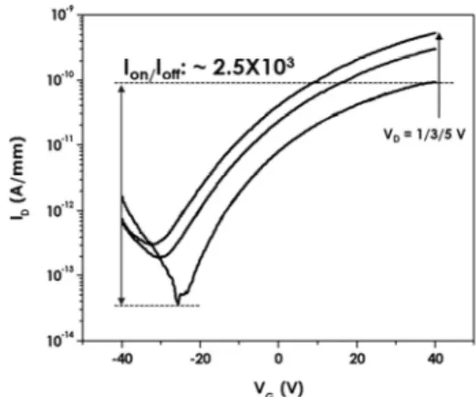
Figure 5 shows the electrical characteristics of the SnS 2 transistor with the Sample 3 channel fabricated by the process preventing damage by the acetone developer. The transistor with Sample 3 channel showed n- type characteristics and a mobility of 2.11x10 -3 cm 2 /Vs, S.S of 11.3 V/decade, and on/off current ratio of 2.5x10 3 . These values are better than those of the SnS 2 transistor fabricated with a device without PVA.
In other words, the damage to SnS 2 by the developer has an adverse
effect on the electrical characteristics of the SnS 2 transistor. Therefore,
there is a need for a process that protects the device from the developer,
and PVA on SnS 2 films played a crucial role in reduction of damage by
the developer.
Giyul Ham · Seokyoon Shin · Juhyun Lee · Namgue Lee · Hyeongtag Jeon 44
Fig. 4. (a) XRD and (b) RAMAN graphs of samples to identify developer effects.
Accordingly, the electrical characteristics of the SnS 2 transistor were improved. However, the electrical characteristics of the transistor using the PVA-protected SnS 2 (Sample 3) channel were also not good compared to the SnS 2 transistor fabricated by the transfer process, 11,12 as the device process to fabricate the SnS 2 transistor was not optimized. To improve the electrical properties of the SnS 2 transistor, it is necessary to optimize the SnS 2 device process by identifying source/drain electrodes that can lower the contact resistance and a gate dielectric that can effectively reduce the Coulomb scattering of the carriers due to the charged defects at the interface.
4. Conclusion
We fabricated the device by depositing source/drain electrodes (Ti/Au, 10/50 nm) after patterning a SnS 2 channel (Sample 2) using a PR-strip process. The fabricated SnS 2 transistor has mobility of 2.6x10 -4 cm 2 /Vs, S.S of 58.1 V/decade, and on/off current ratio of 1.8x10 2 . These results are significantly lower than the transistor characteristics previously reported in the literature. Therefore, we analyzed the reasons for degradation of the properties and found that the SnS 2 channel was damaged by acetone used to remove the PR. To prevent SnS 2 channel
damage by acetone, we added a PVA coating to the SnS 2 channel patterning process. As a result, the damage of SnS 2 was considerably reduced, as confirmed by optical image, XRD, and RAMAN analyses.
The mobility, S.S, and on/off current ratio electrical properties of the transistor with the SnS 2 channel with PVA coating (Sample 3) were 2.11x10 -3 cm 2 /Vs, 11.3 V/decade, and 2.5x10 3 , respectively. These results are approximately 10 times better than those of SnS 2 transistors without a PVA layer. However, the performance of our transistor was not as good as that reported in the literature because the PVA process did not completely protect the SnS 2 thin film from acetone. Therefore, a device process that can completely protect from acetone is required.
Fig. 5. Transfer curves (I ds -V gs ) of the SnS 2 transistor with a channel of Sample 3 in linear and logarithmic scales measured with different V ds
We believe that the performance of SnS2 transistors will be improved through optimized device processes such as selection of source/drain electrodes with low contact resistance to the channel and gate insulators to reduce the scattering of carriers due to charged defects at the interface.
Acknowledgements
This study was supported by a National Research Foundation of Korea (NRF) grant funded by the Korean government (MEST) (NRF- 2014M3A7B4049367).
References
1. Novoselov K S, Geim A K, Morozov S V, Jiang D, Zhang Y, Dubonos S V, Grigorieva I V, Firsov A A ,
"Electri field effect in atomically thin carbon films",
Sicence, 306, pp. 666-669, (2014).
Role of a PVA layer During lithography of SnS2 thin Films Grown by Atomic layer Deposition 45