Vol. 20, No. 7 (2010)
351
†
Corresponding author
E-Mail : [email protected] (W. -G. Jung)
Properties of Aluminum Doped Zinc Oxide Thin Film Prepared by Sol-gel Process
Sung-Hak Yi, Jin-Yeol Kim and Woo-Gwang Jung
School of Advanced Materials Engineering, Kookmin University Seoul, 136-702, Korea (Received June 2, 2010 : Received in revised form June 25, 2010 : Accepted June 25, 2010)
Abstract
Transparent conducting aluminum-doped ZnO thin films were deposited using a sol-gel process. In this study, the important deposition parameters were investigated thoroughly to determine the appropriate procedures to grow large area thin films with low resistivity and high transparency at low cost for device applications. The doping concentration of aluminum was adjusted in a range from 1 to 4 mol% by controlling the precursor concentration. The annealing temperatures for the pre-heat treatment and post-heat treatment was 250oC and 400-600oC, respectively. The SEM images show that Al doped and undoped ZnO films were quite uniform and compact. The XRD pattern shows that the Al doped ZnO film has poorer crystallinity than the undoped films. The crystal quality of Al doped ZnO films was improved with an increase of the annealing temperature to 600oC. Although the structure of the aluminum doped ZnO films did not have a preferred orientation along the (002) plane, these films had high transmittance (> 87%) in the visible region. The absorption edge was observed at approximately 370 nm, and the absorption wavelength showed a blue-shift with increasing doping concentration. The ZnO films annealed at 500oC showed the lowest resistivity at 1 mol% Al doping.Key words
ZnO thin film, Al doping, sol-gel, transmittance, electric conductivity, transparent conducting oxide film.1. Introduction
ZnO, a representative II-VI group compound semicon- ductor with a wide direct band gap (3.37eV) and large exciton binding energy (60meV), is a good candidate as an excellent electronic and photonic material for solar cells,
1)light-emitting diodes,
2)photodetectors
3)and gas sensors.
4)Recently, ZnO has attracted considerable interest as a transparent conducting oxide film (TCO).
5)Transparent con- ducting oxide films have applications in optoelectronic devices, such as solar cells
6,7)and heat mirrors.
8)Doped ZnO film has high chemical stability, abundance in nature, and lower cost than the most currently used transparent conducting oxide materials, indium tin oxide (ITO) and SnO
2. In addition, doping in ZnO increases the film con- ductivity. Higher valence elements, such as indium (In),
9)gallium (Ga),
10)aluminum (Al),
5)can be doping elements in ZnO film. Many techniques have been used to deposit undoped and doped ZnO thin films on a range of substrates, including spray pyrolysis,
10)metal-organic chemical vapor deposition (MOCVD),
3)pulsed laser deposition (PLD),
11)molecular beam epitaxy (MBE),
12)radio frequency magne- tron sputtering,
13)atomic layer deposition (ALD)
14)and sol- gel process.
15)Among them, sol-gel processes have attracted increasing attention because it enables the development of
low cost and simple deposition procedures to obtain high quality transparent conducting oxide films. Although thin films obtained by physical deposition, such as pulsed laser deposition (PLD) and radio frequency magnetron sputtering, exhibit good optical and electrical properties at lower de- position temperatures, the relatively low deposition rate and high equipment cost are significant disadvantages. In this sense, the sol-gel process is a rather efficient technique for depositing aluminum doped ZnO (AZO) films over large areas at low cost for technological applications.
In this study, aluminum doped ZnO films were grown on Si and glass substrates by spin coating using zinc acetate, Al nitrate and 2-methoxyethanol as the precursors, and monoethanolamine (MEA) as the stabilizer. The dopant concentration was varied from 1 to 4 mol%. The film was preheated at 250
oC for 5 min and post-heated in an ambient atmosphere at several temperatures ranging from 400~
600
oC for 30 min. The effects of the doping concentration and thermal treatment on the structure, electrical and optical properties of the ZnO films were investigated. The struc- tural characteristics were examined by XRD and FE-SEM.
The electrical and optical properties were investigated measuring the resistivity and transmittance in the visible and near infrared wavelength region.
2. Experimental Procedure
Al doped ZnO films were prepared using a sol-gel
352 Sung-Hak Yi, Jin-Yeol Kim and Woo-Gwang Jung
process. Zinc acetate dihydrate (Zn(CH
3COOH)
2·2H
2O) was used as the starting precursor material. 2-methoxye- thanol (CH
3OC
2H
4OH) and MEA (H
2NCH
2CH
2-OH) were used as the solvent and stabilizer, respectively. Aluminum nitrate hexahydrate (Al(NO
3)
2·6H
2O) was used as the doping source. The process does not include special hydrolysis.
Zinc acetate dihydrate and aluminum nitrate hexahydrate were first dissolved in mixture of 2-methoxyethanol and MEA solution at room temperature. The precursor solution was mixed thoroughly with a magnetic stirrer. The dopant concentration, as determined by [Al (mol)] / [Al (mol) + Zn (mol)] × 100, was varied from 1 to 4 mol%. MEA was used to increase the solubility of zinc acetate dihydrate.
The MEA to zinc acetate dihydrate molar ratio was 1, and the zinc acetate dihydrate concentration was 0.2 M. The solution was stirred at 60
oC for 2 h until it became clear and homogeneous, and then cooled to room temperature.
The solution was spin coated on a Si substrate and glass in the 1
ststep at 500 rpm for 5 s and in the 2
ndstep at 3500 rpm for 35 s. After spin coating, the film was preheated to 250
oC for 5 min over a hot plate to evaporate the solvent and remove the organic residuals. The coating step was repeated ten times to obtain the desired thickness. After deposition of the last coating, the films were placed into a furnace and annealed in ambient atmosphere at temperatures ranging from 400~600
oC for 30 min.
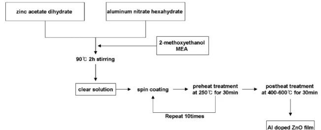
Fig. 1 shows the flowchart showing the procedure for preparing Al doped ZnO. The films were coated on glass substrates for the optical measurements and on Si for examining the morphology and structure. The morphology of the Al doped ZnO films was observed by field emission scanning electron microscopy (FE-SEM, JEOL JSM- 7401F). The crystal structure of the Al doped ZnO films was determined by X-ray diffraction (XRD, Philips xpert system). The optical properties of ZnO films were measured by UV-VIS-NIR spectrophotometry (SHIMADZU, UV-3150).
The electrical resistance was measured using a four point probe method (CHANG MIN TECH CO. LTD., CMT-SR 2000N).
3. Results and Discussion
Fig. 2 shows FE-SEM images of ZnO films. The ZnO films were deposited using a sol-gel process. Fig. 2(a) showed that the undoped ZnO film was porous. Pre- heating the ZnO film to 250
oC resulted in the partial decom- position and removal of the solvent and organic substances from the precursor. The top surface of the ZnO film could be observed clearly. The film thickness can be affected by the viscosity of the solution in sol-gel method with spin-coating and the ionic radius. From the view point of ionic radius, it was expected that the thickness of the Al doped ZnO films would be thinner than the undoped ZnO film, because Al
3+(0.54 Å) has a smaller ion radius than Zn
2+(0.74 Å). However, the cross section images in Fig.
3(b), (c) show that the Al doped and undoped ZnO films have similar thickness (100 nm) with no pores. Al doped and undoped ZnO films were quite uniform and compact.
Fig. 3 shows the XRD pattern of 3 mol% Al doped ZnO films annealed at temperatures ranging from 400
oC to 600
oC for 30 min. Fig. 3 shows three principal peaks, (100), (002) and (101), corresponding to the wurzite lattice.
The 3 mol% Al doped ZnO films had a polycrystalline structure. The XRD pattern showed a strong peak of 34.42
o2 θ due to the ZnO (002) crystal plane and a weak peak at 31.77
oand 36.25
o2 θ due to ZnO (100) and (101) crystal planes, which are in accordance with the JCPDS card no. 36-1451 with lattice constants of a = 3.25 Å and c = 5.21 Å. The intensity of the (002) peak increased with increasing the annealing temperature up to 600
oC (Fig.
3(a)). The (002) peak intensity was increased most sig- nificantly by heating. The other peaks remained relatively
Fig. 1. Outline of the fabrication process for the deposition of Al doped ZnO films.
constant. The increase in (002) peak intensity indicates improvement in the crystalline quality with increasing annealing temperature to 600
oC.
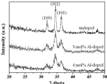
Fig. 4 shows XRD patterns of the ZnO thin films annealed at 600
oC with different Al doping concentra- tions. It is found that the position of (002) peak is shifted to higher angle side for the Al-doped ZnO. The intensity of the (002) peak for the Al doped ZnO films decreased with increasing doping concentration. This indicates that an excess of dopant deteriorates the crystal of the ZnO films, which may be due to the increased compressive stress in the films from the difference in ionic radius between Al
3+(0.54 Å) and Zn
2+(0.74 Å) as well as dopant segregation in the grain boundaries at high doping concentrations.
Fig. 5 shows FE-SEM images of undoped and 3 mol%
Al doped ZnO films annealed at temperatures ranging from 400
oC to 600
oC. The film structure consists of many round shaped particles. The surface morphology of the ZnO films revealed a remarkable transformation. The grains of the undoped and 3 mol% Al doped ZnO films become larger and more densely packed with increasing annealing Fig. 2. Plain view and cross section FE-SEM image of ZnO films fabricated using sol-gel process. (a) Low magnification image showing the undoped ZnO film, (b) cross section image of the undoped ZnO film, (c) cross section image of the 1 mol% Al doped ZnO film.
Fig. 3. XRD patterns of 3 mol% Al doped ZnO thin films deposited on Si substrates using a sol-gel process and annealed at tem- peratures ranging from 400
oC to 600
oC for 30 min.
Fig. 4. XRD patterns of ZnO thin films annealed at 600
oC with
undoped, 3 and 4 mol% Al doping concentration.
354 Sung-Hak Yi, Jin-Yeol Kim and Woo-Gwang Jung
temperature. However, the undoped ZnO films showed denser packing than the 3 mol% Al doped ZnO films. The particle size of the 3 mol% Al doped ZnO film was smaller than that of the undoped ZnO film. The particle size of the Al doped ZnO film decreased with increasing doping concentration. This is because grain growth had been disturbed by compression stresses due to the difference in ionic radius between Al
3+(0.54 Å) and Zn
2+(0.74 Å).
16)These results show that doped ZnO film has poorer crystallinity than the undoped films. This is consistent with the fact observed from the XRD pattern shown in Fig. 4.
Fig. 6 shows the corresponding optical transmittance spectra of ZnO films with different Al doping concentra- tions. The optical transmittance of all ZnO films were
> 87% in the visible and near infrared wavelength regions (glass substrate). The Al doped ZnO films produced in this study by sol-gel process exhibited good optical pro- perties. The transmittance of the blue region was higher than that of the red region. The 4 mol% doped ZnO film showed the highest transmittance. The inside of the film
decreased the light diffused due to increase in grain density.
The absorption edge was observed at approximately 370 nm, which is similar to the band gap of ZnO (3.37eV). The absorption wavelength showed a blue-shift with increasing doping concentration, indicating that the band gap of the ZnO films increases with increasing doping concentration.
This might be due to the Burstein-Moss effect (The bottom of the valance band is full of electrons with increasing doping concentration, and the electron of the valance band requires an excess of energy to excite conduct band.), which describes the blue-shift in the absorption edge of a degenerate semiconductor with increasing carrier concen- tration.
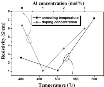
17,18)Fig. 7 shows the electrical properties of the ZnO films as the function of the Al doping concentrations annealed at 500
oC for 30 min and the annealing temperature with Fig. 5. Plain view FE-SEM image of (a) undoped and (b) 3 mol%
Al doped ZnO thin films surface annealed at temperatures ranging from 400
oC to 600
oC.
Fig. 6. The transmittance spectra of the undoped and Al doped ZnO films on glass substrates with different Al doping concentrations.
Fig. 7. Electrical properties of Al doped ZnO films as a function of
the Al doping concentrations (at 500
oC) and annealing temperatures
(at 1 mol% Al).
1 mol% Al doping. The lowest resistivity of Al doped ZnO films was obtained at 1 mol% Al doped ZnO films.
It is usually known that ZnO is a n-type semiconductor in which the major carrier is an electron. A comparison of the Al doped and undoped ZnO films showed that the decrease in electrical resistivity at initial doping concentra- tion might be due to an increase in carrier concentration.
However, the increase in electrical resistivity with further increases in doping concentration might be due to a decrease in the carrier mobility caused by dopant segregation at the grain boundary. In Fig. 7, the ZnO films annealed at 500
oC showed the lowest resistivity at 1 mol% Al doped ZnO films. Consequently, the doping concentration and thermal treatment are important factors in an electrical conductivity of ZnO films.
4. Conclusion
Transparent conducting aluminum doped ZnO thin films were deposited using a sol-gel process. The dopant concen- tration was varied from 1 to 4 mol%. The thickness of the Al doped and undoped ZnO films was similar (100 nm) with no pores. Al doped and undoped ZnO films are very uniform and compact. The (002) peak intensities of the Al doped ZnO films decreased with increased dopant concen- tration due to the increased compressive stress in the films caused by the difference in ionic radius between Al
3+(0.54 Å) and Zn
2+(0.74 Å) as well as dopant segregation in the grain boundaries at high doping concentrations. The grains of undoped and 3 mol% Al doped ZnO films became larger and more densely packed with increasing annealing temperature. The optical transmittance of all ZnO films was
> 87% in the visible and near infrared wavelength region.
The absorption wavelength showed a blue-shift with in- creasing doping concentration. The band gap of the ZnO films increased with increasing doping concentration. The ZnO films annealed at 500
oC showed the lowest resistivity at 1 mol% Al doping. The deposition process in this study requires no expensive and precise vacuum equipment, and allows large scale fabrication of Al doped ZnO films at a relatively low cost. These Al doped ZnO films are expected to have a large number of applications in display, electrical and optical devices.
Acknowledgement
This study was supported by the SRD/ERC program of MOST/KOSEF (R11-2005-048-00000-0) and the Research Program 2009 of Kookmin University in Korea.
References
1. J. B. Baxter and E. S. Aydil, App. Phy. Lett., 86, 053114- 1-3 (2005).
2. N. Saito, H. Haneda, T. Sekiguchi, N Ohashi, I. Sakaguchi and K. Koumoto, Adv. Mater., 6, 418 (2002).
3. S. Liang, H. Sheng, Y. Liu, Z. Huo, Y. Lu and H. Shen, J. Cryst. Growth, 225, 110 (2001).
4. J. Y. Lee, Y. S. Choi, J. H. Kim, M. O. Park and S. Im, Thin Solid Films, 403-404, 553 (2002).
5. G. G. Valle, P. Hammer, S. H. Pulcinell and C. V. Sanrilli, J. Eur. Ceram. Soc., 24, 1009 (2004).
6. T. J. Hsueh, C. L. Hsu, S. J. Chang, P. W. Guo, J. H.
Hsieh and I. C. Chen, Scripta Materialia, 57, 53 (2007).
7. S. J. Tark, M. G. Kang and D. Kim, Kor. J. Mat. Res., 16(7), 449, (2006) (in Korean).
8. G. Alvarez, J. J. Flores, J. O. Aguilar, O.Gómez-Daza, C.
A. Estrada, M. T. S. Nair and P. K. Nail, Solar Energy, 78, 113 (2005).
9. A. E. Morales, M. H. Zaldivar, U. Pal, Optical Materials, 29, 100 (2006).
10. H. Gomez, A. Maldonado and D. R. Acosta, Sol. Energ.
Mater. Sol. Cell., 87, 107 (2005).
11. J. H. Choi, H. Tabata and T. J. Kawai, J. Cryst. Growth, 226, 493 (2001).
12. A. El-Shaer, A. Che Mofor, A. Bakin, M. Kreye and A.
Waag, Superlattice Microst., 38, 265 (2005).
13. Y. J. Cho, A. Park and C. Lee, Kor. J. Mat. Res., 16(7), 445 (2006) (in Korean).
14. A. W. Ott and R. P. H. Chang, Mater. Chem. Phys., 58, 132 (1999).
15. R. Kaur, A. V. Singh and R. M. Mehra, J. Non-Cryst.
Solids, 352, 2335 (2006).
16. Z. Q. Xu, H. Deng, Y. Li, H. Cheng, Mater. Sci. Semicond.
Process., 9, 132 (2006).
17. M. J. Alam and D. C. Cameron, J. Vac. Sci. Technol. A, 19, 1642 (2001).
18. B. E. Sernelius, K. F. Berggren, Z. C. Jin, I. Hamberg and C. G. Granqvist, Phys. Rev. B, 37, 10244 (1988).