332 J. Sens. Sci. Technol. Vol. 29, No. 5, 2020 Journal of Sensor Science and Technology
Vol. 29, No. 5 (2020) pp. 332-335 http://dx.doi.org/10.46670/JSST.2020.29.5.332 pISSN 1225-5475/eISSN 2093-7563
InGaZnO 용액의 농도가 Drop-casting으로 제작된 산화물 박막 트랜지스터의 전기적 특성에 미치는 영향
노은경1 · 유경민2 · 김민회1,2,+
Effect of InGaZnO Solution Concentration on the Electrical Properties of Drop-Cast Oxide Thin-Film Transistors
Eun-Kyung Noh1, Kyeong Min Yu2 and Min-Hoi Kim1,2,+
Abstract
Drop casting, a solution process, is a simple low-cost fabrication technique that does not waste material. In this study, we elucidate the effect of the concentration of a InGaZnO solution on the electrical properties of drop-cast oxide thin-film transistors. The higher the concentration the larger the amount of remnant InGaZnO solutes, which yields a thicker thin film. Accordingly, the electrical properties were strongly dependent on the concentration. At a high concentration of 0.3 M (or higher), a large current flowed but did not lead to switching characteristics. At a concentration lower than 0.01 M, switching characteristics were observed, but the mobility was small.
In addition to a high mobility, sufficient switching characteristics were obtained at a concentration of 0.1 M owing to the appropriate thickness of the semiconductor layer. This study provides a technical basis for the low-cost fabrication of switching devices capable of driving a sensor array.
Keywords: Drop casting, InGaZnO TFT, Electrical performance, Concentration, Semiconductor
1. 서 론
산화물 박막 트랜지스터 (Oxide Thin Film Transistor: OxTFT) 는 별도의 결정화와 도핑 공정 없이 비정질 구조에서 높은 이 동도와 on-off 전류비를 나타내는 장점이 있어서 디스플레이와 센서 구동을 위한 소자로 많이 연구되고 있다.
일반적으로 OxTFT를 제작하기 위해 사용하는 스퍼터링 (sputtering) 은 진공 상태에서 진행되어 불순물의 혼입을 방지할 수 있기 때문에 고품질의 박막을 형성할 수 있지만 재료의 손
실이 크고 속도가 느리며 고가의 진공장비가 필요하므로 생산 단가가 높다[1-2]. 이와 같은 진공 증착 공정과 비교하여서 용 액 공정은 낮은 비용이 필요하고 막의 형성이 간단하고 쉬우며 넓은 면적에 쉽게 형성이 가능하다는 장점을 갖는다[3-4]. 용액 공정 방법 중 하나인 spin-coating은 넓은 면적에 균일한 박막을 형성할 수 있지만, 재료의 소모가 많고 전 영역에 걸쳐 박막을 형성하기 때문에 추가적인 패터닝 공정이 요구되는 것에 비하 여 inkjet이나 drop-casting의 경우에는 직접 패터닝이 가능하므 로 일반적인 포토리소그래피를 통한 패터닝 공정을 생략할 수 있다는 장점이 있다[5].
이러한 용액 공정을 적용한 산화물 반도체는 금속 전구체 (metal precursor)를 용매에 분산시킨 후 박막을 형성하고 열 을 가하여 용매를 증발시킨 뒤 금속-산소 결합을 통해 산화물 박막을 형성하는 과정을 거친다. 용액 공정을 이용한 산화물 반도체 개발은 무엇보다도 간단하게 전구체의 비율과 농도, 박 막 형성 방법 등의 조건들을 조절하는 것이 용이하기 때문에 다양한 형태의 산화물 박막의 제조가 가능하여 진공 공정에서 시도 해보기 어려운 다양한 방법들을 활용하여 연구가 진행 중에 있다.
본 논문에서는 drop-casting 방식에 사용되는 InGaZnO 용 액의 농도가 OxTFT의 전기적 특성에 미치는 영향을 조사하 고 최적화된 전기적 특성을 위한 농도를 제시한다. 먼저, 실험
1한밭대학교 창의융합학과(Department of Creative Convergence Engineering, Hanbat National University)
N13-909, Hanbat National University, 125 Dongseodaero, Yuseong-gu, Daejeon 305-719, Korea
2한밭대학교 산학협력단 인쇄전자 3D 프린팅 공학 연구소 (Research
Instite of Printed Electronics & 3D Printing, Industry University Cooperation Foundation, Hanbat National Unversity)
125 Dongseodaero, Yuseong-gu, Daejeon, 305-719, Korea
+Corresponding author: [email protected]
(Received : Sep. 4, 2020, Revised : Sep. 8, 2020, Accepted : Sep. 9, 2020)
This is an Open Access article distributed under the terms of the Creative Commons Attribution Non-Commercial License(https://creativecommons.org/
licenses/by-nc/3.0/) which permits unrestricted non-commercial use, distribution, and reproduction in any medium, provided the original work is properly cited.
Effect of InGaZnO Solution Concentration on the Electrical Properties of Drop-Cast Oxide Thin-Film Transistors
333 J. Sens. Sci. Technol. Vol. 29, No. 5, 2020 방법에서 drop-casting으로 OxTFT를 제작하는 방법을 자세하
게 나타내었다. 결과 및 고찰에서는 InGaZnO 농도에 따른 박 막의 두께와 제작된 트랜지스터의 전기적 성능을 제시하였다.
해당 특성을 분석하여서 최적화된 트랜지스터의 성능을 위한 농도를 제시하였다.
2. 연구 방법
Fig. 1 은 Si 기판 위에 drop-casting 을 이용하여 InGaZnO 층 을 형성한 후 코팅된 InGaZnO 박막 위에 쉐도우 마스크를 통 해 Al 전극이 열 증착된 산화물 반도체의 단면도이다. 먼저, SiO
2가 200 nm 증착된 Si 기판을 Acetone과 IPA에 각각 15분 동안 초음파 세척한 후 15분 동안 UV 처리를 해주었다. InGaZnO 용 액은 indium nitrate(III) hydrate, gallium nitrate(III) hydrate, zinc nitrate hydrate 를 2-methoxyethanol과 섞어 각각 0.5 M, 0.3 M, 0.1 M, 0.01 M, 0.007 M, 0.005 M 로 제작하였고, 원자 간 몰 비 율은 In(4):Ga(3):Zn(2)로 조절하였다. 기판 위에 다양한 농도의 InGaZnO 용액을 drop 하여 하나의 droplet을 형성한 후 110
oC 에서 10분간 용매를 제거하고 500
oC에서 3시간 동안 열처리 해 주었다. 이때, 형성된 박막의 두께는 두께 측정 장비(Dektak-8 Surface Profiler)를 이용하여 측정되었다. 반도체층인 InGaZnO 위에 Al을 120 nm 열증착하여 전극을 형성하였다. 채널의 길이 는 200 µm, 폭은 1000 µm로 제작하였다. 제작된 소자들은 off 전류의 개선을 위해 S/D 전극 증착 후 200
oC에서 1시간 동안 열처리하였다. 대기 조건에서 반도체 특성 분석기 (HP 4155A) 를 사용하여서 전기적 특성을 측정하였다.
3. 결과 및 고찰
InGaZnO 용액은 소자마다 약 1 ml의 양으로 InGaZnO droplet 을 형성하였다. Drop-casting 공정으로 형성된 droplet은 가장 자리 용매의 증발이 중앙 부위의 증발보다 빠르게 일어나고,
droplet의 내부에서는 이러한 증발률의 차이에 의하여 중앙에 서 가장자리의 방향으로 용질의 유동이 발생한다. 이때, 용질 들이 가장자리에 모여들면서 coffee-ring과 같은 형상으로 박막 이 형성되는 것을 Fig. 2(a)를 통해 확인하였다[6]. 하지만 InGaZnO 의 농도가 높아질수록 droplet의 접촉각이 증가하게 되어 상대 적으로 가장자리의 증발률이 감소하게 된다[7]. 이는 결과적으 로 coffee-ring 효과를 줄이지만 중앙으로 용질이 뭉쳐지게 되 어 박막의 표면에 얼룩과 같은 불균일한 박막을 형성한다는 것 을 Fig. 2(b)의 현미경 사진을 통하여 알 수 있다. 이러한 현상 은 형성된 두께를 용액이 코팅되어있지 않은 기판에서부터 박 막의 중심부까지 알파스탭으로 측정한 Fig. 2(c)에서 명확하게 확인할 수 있다. 가장자리에 해당하는 360 µm 영역에서부터 750 µm까지는 급격히 높이가 증가하는 것을 볼 수 있으며, 0.005 M의 농도에서는 중심부에서 평탄한 두께 25 nm를 가지 지만 0.3 M의 농도에서는 모든 영역에서 불균일한 박막을 갖 는다. 따라서 coffee-ring 효과의 영향을 많이 받지 않는 InGaZnO 박막의 중심부에 채널이 위치하도록 source/drain 전극을 형성 하여 전기적 특성을 확인하였다.
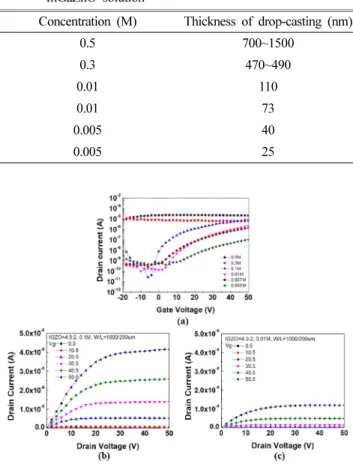
InGaZnO 의 농도에 따른 OxTFT의 transfer curve을 Fig. 3(a) 에 나타내었다. 반도체층의 두께는 전하밀도와 관련되어 있으 며, InGaZnO 박막 중심부 두께의 평균값을 계산하여 Table 1 에 제시하였다. 0.3 M 이상의 농도의 용액으로 제작된 반도체 박막에서는 11 mA의 drain 전류가 흐르지만 측정 범위(V
g=-20 V ~ 50 V) 내에서는 V
th특성이 나타나지 않았다. 이는 반도체 층 의 두께가 너무 두껍게 되면 높은 전하 밀도로 인해 Negative V
th특성을 나타내게 되기 때문이다[8-10]. 따라서 drop-casting Fig. 1. The solution process for oxide TFT: InGaZnO solution Drop
on the Si/SiO
2substrate. Al electrode deposition using vac- uum deposition on the dropped InGaZnO solution.
Fig. 2. Optical microscopy image of surface of InGaZnO thin film;
(a) 0.005 M (b) 0.3 M and (c) Thickness of InGaZnO thin
film
Eun-Kyung Noh, Kyeong Min Yu and Min-Hoi Kim
J. Sens. Sci. Technol. Vol. 29, No. 5, 2020 334 으로 제작된 OxTFT의 향상된 전기적 특성을 얻기 위해서는 적 절한 두께의 박막을 형성하는 낮은 몰 농도의 용액이 필요하다.
본 실험 조건에서는 0.1 M에서 형성된 110 nm의 두께가 높은 전하이동도를 가지면서 0 V 근처에서 V
th를 가지게 되어 가장 적합한 두께를 나타낸다. 0.01 M 이하의 낮은 농도에서는 스위 칭 특성이 나타나지만 on 전류가 감소한다. 반도체층의 두께가 너무 얇으면 전하 이동도를 확보할 수 있는 균일한 박막이 형 성되지 않기 때문에 이동도의 감소를 나타낸다. Fig. 3(b)와 (c) 에서는 각각 0.1 M과 0.01 M에서의 output curve를 나타낸다.
제작된 소자들은 누설전류가 발생하지 않는 것을 확인할 수 있 는데, 이것은 drop-casting 공정의 직접 패터닝에 의한 결과이다 [11]. I
ds-V
ds특성에서 일반적인 InGaZnO 반도체의 동작을 확인 할 수 있는데, 두께가 증가할수록 pinch-off된 후에 포화영역에 서 전류의 증가를 보인다.
Fig. 4(a) 에서는 InGaZnO 용액의 농도가 0.1 M에서 0.005 M 로 낮아질수록 문턱전압은 3.4 V에서 20.5 V까지 양의 방향으 로 이동한다. 이는 위에서 설명한 반도체 층의 두께에 따른 전 하 밀도의 변화와 일치한다. 0.3 M 이상의 농도에서는 과도한 두께의 박막으로 인하여 스위칭 특성이 나타나지 않아 측정 범 위 내에서 문턱전압을 확인할 수 없었다. 반면, Fig. 4(b)의 이동
도는 용액의 농도가 0.1 M에서 0.005 M로 낮아질수록 0.09 cm
2V
-1s
-1에서 0.003 cm
2V
-1s
-1으로 감소하는데, 이는 얇은 박막 내 에서의 불안정한 박막의 막질에서 발생하는 반도체층 내의 결함 들에 trap 되는 캐리어에 의해서 전도도에 기여하는 캐리어 수가 감소되기 때문이다[12]. 결과적으로 스위칭 특성이 나타나는 InGaZnO 용액 중 가장 농도가 높은 0.1 M에서 0.09 cm
2V
-1s
-1로 가장 높은 이동도를 보였으며 4.17×10
-6A 이상의 높은 온 전 류를 얻을 수 있었다.
4. 결 론
재료의 낭비 없이 반도체 층을 간단하게 형성할 수 있는 drop- casting 을 사용하여 산화물 박막 트랜지스터를 제작하였다. InGaZnO 용액의 농도에 따른 전기적 특성의 변화를 알아보았다. 0.3 M 이상의 농도에서는 매우 두꺼운 박막이 형성되어 높아진 전하 밀도로 인하여 V
th가 음의 방향으로 이동하기 때문에 스위칭 특 성이 나타나지 않았고, 그 이하의 농도에서의 얇은 박막은 스위 칭 특성과 이동도를 나타내었다. 0.1 M에서 110 nm로 가장 적 절한 두께의 박막을 형성하여 3.37 V의 V
th를 나타내며 0.09 cm
2V
-1s
-1의 가장 높은 이동도를 보였다. 본 연구의 결과는 용 액의 낭비를 줄여 저비용으로 센서를 구동할 수 있는 소자의 제 작을 위한 기술적 기초를 제공한다.
감사의 글
이 논문은 2018년도 정부(교육부)의 재원으로 한국연구재단의 지원을 받아 수행된 기초연구사업임(No. 2018R1A6A1A03026005) Table 1. Thickness of thin film corresponding to the concentration of
InGaZnO solution
Concentration (M) Thickness of drop-casting (nm)
0.5 700~1500
0.3 470~490
0.01 110
0.01 73
0.005 40
0.005 25
Fig. 3. Electrical properties; (a) transfer curve of various concen- tration of InGaZnO. (b) output characteristic curve of 0.1 M (c) output characteristic curve of 0.01 M InGaZnO.
Fig. 4. Changes in properties according to InGaZnO concentration
(a) Threshold voltage, (b) mobility, (c) on current
Effect of InGaZnO Solution Concentration on the Electrical Properties of Drop-Cast Oxide Thin-Film Transistors
335 J. Sens. Sci. Technol. Vol. 29, No. 5, 2020
REFERENCES