P1-124 /D. -H. Son
IMID 2009 DIGEST •
Abstract
We studied the solution processes of IGZO thin films and investigated the electrical characteristics of thin film transistor (TFT) with sol-gel processed InGaZn-oxide active semiconductor layer. In particular, the effect of composition variation and post annealing temperature were studied by using solutions having various metal cation ratios to optimize transistor performance.
1. Introduction
Nowdays, n-type metal oxide semiconductors have attracted attention as potential candidates for active-matrix organic light-emitting diode (AMOLED) backplane application, due to many advantages, such as their good electrical performance and reliability.[1] They are also possible to fabricate large-size area features with a good uniformity, high stability, transparent and low processing cost, comparable to a-Si TFT. For that reason, many metal oxide semiconductors using ZnO, AlZnSnO, InZnO, ZnSnO and InGaZnO thin films have reported for active-channel materials in TFTs.[2~4] In general, above mentioned metal oxide layers are deposited in the vacuum process such as the rf/dc sputtering, PLD (pulsed laser deposition). These vacuum deposition methods require expensive equipments and result in high manufacturing cost.
Very recently, there are some reports deals with solution processed ZnO based TFT.[5,6] The most notable aspect of chemical solution process is that spin-coating deposition offers a simple, easy and low cost processing alternative to vacuum processing. In this work, we made various IGZO transistors having different compositions, and studied their
electrical properties such as field effect mobility, on/off ratio, threshold voltage and bias stability. Also, we have tried to find out the optimized conditions at different post annealing temperature, different metal precursor ratios, etc.
2. Experimental
The IGZO solution was prepared by dissolving indium nitrate hydrate [In (NO3)3 ·xH2O], gallium
nitrate hydrate [Ga (NO3)3 ·xH2O] and zinc acetate [(CH3CO2)2Zn] metal precursor in acetyl acetone at
various molar ratio. Then, monoethanolamine (MEA) and acetic acid were added to the solution. The solutions become clear and homogeneous after stirring for 24 hours. Heavily boron (p+) doped Si wafer with 100nm thermally grown SiO2 serve as the back gate
and part of the gate-dielectric stack of the TFT, respectively. The SiO2/Si wafer was used as a
substrate after cleaning with acetone, methanol and DI water in sequence. The resulting IGZO solution was formed on the SiO2/Si substrate by spin coating
method. IGZO thin films were annealed at various temperatures (600 , 500 , 350 ) in oxygen or 4% H2/N2 gas mixture ambient. The source and drain Al
electrodes were deposited on the IGZO layer through a shadow mask.
3. Results and discussion
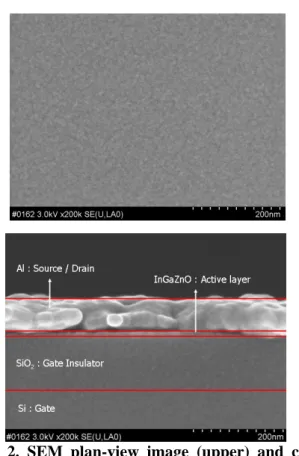
Figure 2 (upper) and (lower) show plan view, and cross sectional images of an IGZO TFT which was fabricated with metal precursors [In(0.1M): Ga(0.1M): Zn(0.1M) = 2: 1: 1] and annealed at 600 for 1hour. SEM images clearly show that IGZO film is
Chemical Solution Deposition of InGaZnO Thin Films As
Active Channel Layers of Thin-Film Transistors
Dae-ho Son
1, Jung-Hye Kim
2, Dae-Hwan Kim
*1, Shi-Joon Sung
1,
Eun Ae Jung
1, Jin-Kyu Kang
1, Ki-Ryong Ha
21Public & Original Technology Research center, DGIST, Daegu, Korea
*Tel.:82-53-430-8429, E-mail: [email protected]
P1-124 /D. H. Son
• IMID 2009 DIGEST
uniform and smooth. Cross sectional image shows that ~10nm-thick IGZO layer were prepared on above mentioned experimental conditions.
Fig. 2. SEM plan-view image (upper) and cross-sectional image (lower) of IGZO [2:1:1 (0.1M)] post annealed at 600
Figure 3 shows the transfer characteristics of the IGZO TFTs (W/L = 1000µm/ 40µm) coated with solutions having various metal precursor molar ratios, and annealed at 600 for 1hour in oxygen ambient. All TFTs except the IGZO TFT [2:1:1 (0.1M)] show good operating property, with high on/off ratio of ~ 106. The electrical parameters including the saturation field effect mobility and threshold voltage were derived from a linear fitting to the plot of the square root of drain current versus gate voltage. Following equation is the general expression for the operation of a field effect transistor in the saturation region: [7]
2
)
)(
2
(
G th sat i DV
V
L
WC
I
=
µ
−
where W is the channel width, L is the channel length, Ci is the capacitance per unit area of the gate insulator,
VG is the gate voltage, ID is the drain to source current,
and Vth is the threshold voltage of TFT.
Fig. 3. Transfer characteristics of sol-gel process IGZO TFTs (W/L = 1000µm/ 40µm) with VDS=20V that were made of different metal precursor mole ratios at 600
The filed effect mobilities (µFE) of IGZO [3:2:2
(0.1M)], IGZO [3:1:1 (0.1M)], IGZO [2:1:1 (0.2M)] and IGZO [2:1:1 (0.1M)] TFTs in the saturation
region were extracted as 0.6, 0.1, 0.003 and 0.09 cm2/V·s. The mobility of the transistor formed
IGZO [3:2:2 (0.1M)] was significantly improved compared to the other TFTs but threshold voltage are shifted to the negative direction.
Figure 4 shows the transfer characteristics of the IGZO TFTs (W/L = 1000µm/ 40µm) coated with solutions having various metal precursor molar ratios, and annealed at 500 for 1hour in oxygen ambient.
Fig. 4. Transfer characteristics of sol-gel process IGZO TFTs (W/L = 1000µm/ 60µm) with VDS=20V that were made of different metal precursor mole ratios at 500
The field effect mobilities (µFE) of IGZO [3:1:1
(0.1M)], IGZO [2:1:2 (0.1M)], IGZO [2:1:1 (0.1M)], and IGZO [3:2:2 (0.1M)] TFTs in the saturation
P1-124 /D. -H. Son
IMID 2009 DIGEST •
cm2/V·s. In our experiment, high indium mole ratio shows better field effect mobility, which is consistent with the previous study reporting that the fraction of In2O3 content primarily determines transistor mobility.
[8]
Fig. 5. Transfer characteristics of sol-gel process IGZO TFTs (W/L = 1000µm/ 60µm) with VDS=20V that were made of different metal precursor mole ratios for 2 hours at 350
Figure 4 show the transfer characteristics of the IGZO TFTs (W/L = 1000µm/ 60µm) coated with solutions having various metal precursor molar ratios, and annealed at 350 for 1 hour in oxygen and 2 hours in 4% H2/N2 gas mixture ambient. The filed effect
mobilities (µFE) of IGZO [3:1:1 (0.1M)], IGZO [2:1:1
(0.1M)] and IGZO [2:1:2 (0.1M)] TFTs in the saturation region were extracted as 0.07, 0.001 and 0.0001 cm2/V s. We also fabricated the IGZO TFTs at 350 for 2 hour in oxygen ambient but these TFTs have poor electrical properties of low on/off ratio and mobility. But the IGZO TFT sequentially annealed at 350 O2 (1h) – 4% H2/N2 (1h) show greatly
improved electrical performances. It is well known that hydrogen atoms, expected to occupy the interstitial site in the ZnO crystal from a consideration of the Bohr radius, are promising dopants acting as donors.[9] That is to say, interstitial hydrogen atoms in ZnO crystal act as shallow n-type dopants and as a result the films conductivity increases. We believe that the solution-processed IGZO TFT showing reasonable electrical performance at low annealing temperature of 350 is promising result for low temperature printed electronics. However, it requires further extensive studies to improve electrical characteristics of TFTs, lower annealing temperature, and shorten annealing time.
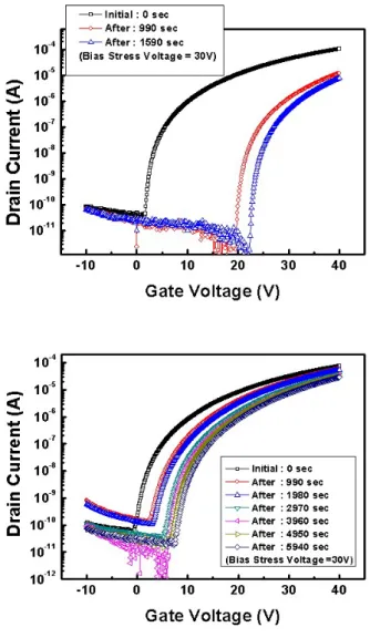
We also examined the operational stability of lithographically patterned the IGZO TFT (3:1:1 at 500 ), including a simple passivation layer (photo resistive: AZ 7210). After forming IGZO films, the channel regions were patterned by wet-etching process using Al-12SK and then a lift-off process to form source and drain electrodes was conducted. Finally, to make passive layer, photo resistive layer was spun and patterned.
Fig. 6. Bias-stress test results of sol-gel process IGZO TFTs (W/L = 1000µm/ 60µm, Vd=20V) under the +30V gate bias voltage without passivation layer (upper) with photo restive layer (lower)
Figure 6 shows the turn-on voltage shift under a 30 V gate bias. The first curve(left) in the figure 6(upper) was measured before the gate bias stress voltage was applied, the second curve(center) after the gate bias stress have been applied for 990 s and the third curve
P1-124 /D. H. Son
• IMID 2009 DIGEST
(right) after the gate bias for 1590 s. As shown in Figure 6 (upper), the application of gate stress voltage for 1590 s led to a significant Vth shift (> 20 V) in the
IGZO TFT without a passivation layer. However, stability of the photo-resist passivated IGZO TFT shifted about 3V by the gate bias stress voltage for 990s, as shown in Figure 6 (lower). The photo-resist passivated device has shown smaller positive shift than the non-passivated device. The photo-resist passivation of TFT shows that, although the photo-resist passivation improved the gate bias stability, it is not sufficient to channel passivation, which is probably due to the polar properties of organic PR. This results can be understood by considering environment related reactions with the back surface of the IGZO channel areas and electron or hole charges are trapped in the between the active layer and the gate insulator.[3,10,11] More studies with non-polar capping layers for interface traps between the active layer and the gate insulator in the active layer formation process are required.
4. Summary
In this study, InGaZnO thin films to improve electrical properties as an active layer in TFT at the different metal precursor mol ratio and post annealing temperature were prepared. Also, we successfully manufactured IGZO TFTs which were annealed at low temperature (350 ). Low temperature annealing process provides that the solution-processed IGZO TFTs are promising device for the high performance driving device of flexible electronics.
Acknowledgement
This work was supported by the DGIST Basic Research Program of the MEST (Ministry of Education, Science & Technology).
5. References
1. Hisato Yabuta, et al, Appl. Phys. Lett. 89, 112123 (2006)
2. Doo-Hee Cho, et al, Appl. Phys. Lett. 93, 142111 (2008)
3. Sung Kyu Park, et al, Electrochem. Solid-State Lett. 12 H256 (2009)
4. Yu-Lin Wang, et al, , Appl. Phys. Lett. 90, 232103 (2007)
5. Gun Hee Kim, et al, J. Electrochem. Soc. 156, H7 (2009)
6. Gun Hee Kim, et al, Appl. Phys. Lett.94, 233501 (2009)
7. Dieter K Schroder, Semiconductor material and device Characterization. 2nd ed”, Wiley (1998) 8. Hideo Hosono, J. of Non-Crystalline Solids 352,
851 (2006)
9. Shigemi Kohiki, et al, Appl. Phys. Lett. 64, 2876 (1994)
10. Donghun Kang, et al, Appl. Phys. Lett. 90, 192101 (2007)
11. Jin-Seong Park, et al, Appl. Phys. Lett. 92, 072104 (2008)