P1-4 / K. H. Kim
• IMID 2009 DIGEST
Abstract
We have fabricated solution-processed zinc-tin oxide thin film transistors (TFTs) and simple circuits on glass substrates. We report a solution-processed zinc-tin oxide TFTs on silicon wafer with mobility greater than 9 cm2/V • s (W/L = 100/5 μm)
and threshold voltage variation of less than 1 V after bias-stressing. Also, we fabricated solution-processed zinc-tin oxide circuits including inverters and 7-stage ring oscillators fabricated on glass substrates using the developed zinc-tin oxide TFTs.
1. Introduction
The high performance transparent oxide TFTs is typically fabricated by using vacuum process such as sputtering or pulsed laser deposition. However, vacuum-deposition methods require expensive equipments and thus high manufacturing costs. Solution-processed oxide TFTs can enable low-cost manufacturing approaches, such as spin-coating and ink-jet printing. In recent years, many researchers have reported relatively high mobility solution-processed multicomponent transparent oxide semiconductor TFTs such as zinc-oxide (ZnO), indium-gallium–zinc-oxide (IGZO), indium-zinc-oxide (IZO), and zinc-tin-indium-zinc-oxide (ZTO) [1-5]. However, most of publications regarding solution-processed transparent oxide TFTs have shown electrical characteristics of relatively long channel length devices (L = 50 ~ 120 μm) from shadow mask patterned electrodes, which may have less contact resistance and natural built-in carrier effects in channel area. In this paper, we demonstrate lithographically patterned high performance solution-processed amorphous ZTO (a-ZTO) TFTs (W/L = 100 μm/5 μm) with mobility greater than 9 cm2/V-s and their applications for display backplane and integrated circuits[6-7].
(a)
(b)
2. Experimental
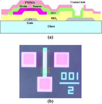
Fig. 1 shows a cross-sectional images and optical micrograph of fabricated a-ZTO. For this paper, transistors were fabricated on heavily doped p-type Si wafers with a 200 nm thermally grown SiO2 gate
dielectric layer. On the other hand, integrated circuits were fabricated on soda-lime glass. In case of glass, Chromium (Cr) was deposited by sputtering and patterned by wet etching to form the gate electrode and sputtered silicon dioxide (SiO2) was patterned by
wet-etching to form the via contact.
The a-ZTO solution was prepared by dissolving 0.07 M SnCl2 [formula weight (FW) of 189.6,
Aldrich] and 0.07 M ZnCl2 (FW of 136.3, Aldrich)
powders in acetonitrile at equal molar ratio. To
Solution-Processed Zinc–Tin Oxide Thin-Film Transistors for
Integrated Circuits
Kwang Ho Kim, Sung Kyu Park*, Yong-Hoon Kim, Hyun Soo Kim, Min Suk
Oh, and Jeong-In Han
Semiconductor and Information Display Research Division, Korea Electronics Technology Institutes, Kyunggi 654-801, Korea
Phone: +82-31-789-7412, E-mail: [email protected]
Keywords : Zinc-Tin Oxide, Thin-Film Transistors, Integrated Circuits
Fig. 1. Schematic diagram of cross-sectional images (a) and optical micrograph(b) of fabricated a-ZTO.
P1-4 / K. H. Kim
IMID 2009 DIGEST • facilitate the dissolving process zinc-tin oxide solution
was stirred at a room temperature for 30 m. The a-ZTO film thicknesses were adjusted to about 30–40 nm from the spinning process with 4000 rpm. After spinning, the a-ZTO films were baked at a temperature of 200°C 10 min. After baking, to avoid a large leakage current, the channel areas were isolated by the wet-etching process using diluted HF (HF:distilled water = 1:500). After ehching, the a-ZTO films were annealed at a temperature of 500°C for 1 h and cooled down to room temperature.
After forming a-ZTO films, Indium-Zinc Oxide (IZO, 100 nm) deposition was carried out using a RF sputter and then followed by a lift-off process to yield source and drain electrodes. The source and drain electrodes formed a channel measuring approximately 100 μm in width and 5–50 μm in length. The poly methyl methacrylate (PMMA, MicroChem A4) was used as a channel passivation layer. All the electrical measurements were performed using a Keithley 4200 SCS semiconductor characterization system in a dark air ambient at room temperature.
3. Results and discussion
Fig. 1 shows a cross-sectional image of the fabricated device of the a-ZTO film on a glass substrate. The inset of Fig. 1 demonstrates an optical micrograph of the fabricated device (W/L = 100/5 μm). Fig. 2 indicates a representative transfer and output characteristics of the sol–gel processed a-ZTO TFT (W/L = 100/5 μm). The a-ZTO TFT sample on a Si wafer have a mobility of 9 cm2/V-s, a threshold
voltage of -1 V, and a subthreshold slope of 1.5 V/decade. After 3600 sec, bias stressing (Ids=10 µA, Vgs= 20 V), the devices with PMMA passivation have Fig. 2. Representative transfer and output
characteristics of the sol–gel processed a-ZTO TFT (W/L = 100/5 μm) on s Si wafer.
Fig. 3. Optical micrograph of solution processed zinc-tin oxide TFT inverter circuit and 7stage ring oscillator on a glass substrate.
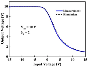
Fig. 4. Measurement results and Aimspice simulation results of the inverter circuit with L = 5 μm, Wload = 50 um, and Wdrive = 100 μm, measured under the voltage supply of Vdd = +10 V.
P1-4 / K. H. Kim
• IMID 2009 DIGEST
shown relatively stable threshold voltage variation (< 1 V). Fig. 3 show optical micrograph of solution processed zinc-tin oxide TFT inverter circuit and 7-stage ring oscillator on a glass substrate. Fig. 4 show dc characteristics and Aimspice simulation[8] results of an inverter with Wload = 50 μm and Wdrive = 100 μm,
measured under voltage supply of Vdd = +10 V. The
inverter beta ratio and gain are > 2 and > 1.2, respectively. As shown in Figure 4, the simulated and experimental results are well matched. The 7-stage ring oscillators are under measuring now and will be presented.
4. Conclusion
In summary, using the soluble zinc-tin oxide, we have fabricated solution-processed a-ZTO TFTs and simple circuits on glass substrates. The solution-processed oxide TFTs can provide a path for producing high-performance TFTs with simple fabrication process. These results demonstrate the simple and efficient solution-process can be a good candidate for the fabrication of large area display backplane and drive circuits.
5. References
[1] S. K. Park, Y. H. Kim, H. S. Kim, and J. I. Han, Electrochem. Solid-State Lett., 12, H256 (2009).
[2] H. Cheng, C. Chen, and C. Tsay, Appl. Phys. Lett., 90, 012113 (2007).
[3] G. H. Kim, H. S. Shin, B. D. Ahn, K. H. Kim, W. J. Park, and H. J. Kim, J. Electrochem. Soc., 156, H7 (2009).
[4] P. Gorrn, F. Ghaffari, T. Riedl, and W. Kowalsky, Solid-State Electrinics, 53, 329 (2009).
[5] P. Gorrn, P. Holzer, T. Riedl, W. Kowalsky, J. Wang, T. Weimann, P. Hinze, and S. Kipp, Appl. Phys. Lett., 90, 063502 (2007).
[6] M. Ofuji, K. Abe, H Shimizu, N. Kaji, R. Hayashi, M. Sano, H. Kumomi, K. Nomura, T. Kamiya, and H. Hosono, IEEE Electron Device Lett., 28, 273(2007).
[7] J. Sun, D. A. Mourey, D. Zhao, S. K. park, S. F. Nelson, D. H. Levy, D. Freeman, P. C. Corvan, L. Tutt, and N. Jackson, IEEE Electron Device Lett.,
29, 721(2008)