47-3 / Y.-H. Kim
• IMID 2009 DIGEST
Abstract
Solution-processed indium-gallium-zinc-oxide thin-film transistors were fabricated by sol-gel method. By a combinatorial study of InGaZnO multi-component system, optimum molar ratio of In, Ga, and Zn has been selected. By adjusting the In:Ga:Zn molar ratio, TFTs with field-effect mobility of 0.5 ~ 1.5 cm2/V-s, threshold
voltage of -5 ~ 5 V, and subthreshold slope of 1.5 ~ 2.5 V/decade were achieved.
1. Introduction
Oxide semiconductor based thin-film transistors (TFTs) are of great interest in the field of active-matrix driven displays due to their relatively high carrier mobility and simple architecture compared to polycrystalline silicon TFTs. The oxide semiconductors can be deposited by means of conventional vacuum deposition methods such as sputtering, chemical vapor deposition and atomic layer deposition [Ref]. In recent, solution-processed oxide TFTs have been reported which has the potential advantages such as non-vacuum process and low-cost manufacturing employing printing technologies [1-3].
In multi-component systems such as InGaZnO semiconductor, combinatorial research is definitely needed to find out the role of each component and the effect on the electrical properties. The combinatorial approaches therefore may give a rapid landscape for understanding the electrical properties of the TFTs. Up to now, a few papers have reported concerning the combinatorial research of vacuum deposited oxide TFTs [4]. However, combinatorial study on solution-processed InGaZnO TFTs has yet been reported.
In this report, to extract the optimum In:Ga:Zn molar ratio and fabrication conditions for solution-processed InGaZnO TFTs, we have performed
combinatorial study on InGaZnO TFTs having relatively short channel length (L~ 20 µm).
2. Experimental
For InGaZnO TFT fabrication, heavily doped p-type silicon wafer has been used as the substrate and also as a common gate electrode. Thermally grown silicon dioxide (thickness of 200 nm) was served as a gate insulator. The InGaZnO solution was prepared by mixing In(NO3)3H2O, Ga(NO3)3H2O, and Zn(Ac)2H2O
powders in 2-methoxyethanol mixed with mono-ethanolamine at various In:Ga:Zn molar ratio. Acetic acid was added into the mixed solution as a stabilizer. The InGaZnO solution was spun over the gate insulator and spin coated to form 30 ~ 40 nm-thick films.
After the spin coating, the oxide films were annealed in a furnace at the temperature of 500°C for
1 hour. As source/drain electrode 100 nm-thick Al was deposited by thermal evaporation and patterned by lift-off process. The channel width and length of the TFT device were 200 and 20 µm, respectively. For
device passivation and channel isolation, poly(methyl methacrylate) (PMMA) was spin coated over the sample and patterned. Then InGaZnO layer was patterned by a wet etching process using PMMA layer as a resist. Figure 1 displays schematic diagrams and optical image of fabricated InGaZnO TFTs.
Sol-Gel Processed InGaZnO Oxide Semiconductor
Thin-Film Transistors for Printed Active-Matrix Displays
Yong-Hoon Kim, Sung Kyu Park, Min-Suk Oh, Kwang-Ho Kim, Jeong-In
Han
Flexible Display Research Center, Korea Electronics Technology Institute, Seongnam,
Gyeonggi 463-816, Korea
Phone: +82-31-789-7413, E-mail: [email protected] Keywords: sol-gel, InGaZnO, thin-film transistor
47-3 / Y.-H. Kim
IMID 2009 DIGEST •
Fig. 1. Schematic cross-section diagram and optical microscope image of InGaZnO TFTs.
3. Results and discussion
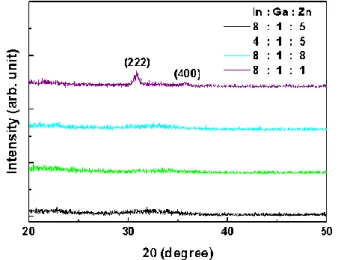
The results of grazing incident X-ray diffraction patterns of InGaZnO films with various molar ratios are displayed in Fig. 2. As illustrated, high In molar ratio (In/(In+Ga+Zn) > 80%) facilitates formation of polycrystalline structure while amorphous state is observed in lower In molar ratios. The peaks detected in polycrystalline films were (222) and (400) peaks of In2O3.
Fig. 2. Grazing incident X-ray diffraction pattern of sol-gel processed InGaZnO thin films with various molar ratios.
Figure 3 shows the transfer characteristics of the solution-processed InGaZnO TFTs with various In:Ga:Zn molar ratios (6:1:3, 4:1:5, 2:1:7, 1:1:8, 0:1:9).
Fig. 3. Effects of In:Ga:Zn molar ratio on the transfer characteristics of a-InGaZnO TFTs with fixed Ga content.
As shown in this figure, it is clear that In-rich (molar ratio > 60%) devices typically show large negative turn-on voltage (Von) and larger drain current.
The significantly negative-shifted Von is due to high
carrier concentration in the InGaZnO channel layer. The negative-shifted Von as well as the increased drain
currents with increasing In molar ratio is well consistent with our Hall measurement results (not shown here) and previous reports. The increased drain currents and carrier concentrations can be explained by enlarged In 5s orbital in the bottom of conduction band from additional In3+ ions incorporation into
InGaZnO4 structure, resulting in denser or larger InO6
octahedra structure [5,6].
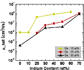
Figure 4 demonstrates the combinatorial effects of In, Ga, and Zn on the field effect mobility of solution-processed InGaZnO TFTs. As shown in figure, it is apparent that field-effect mobility of 0.5 ~ 1.5 cm2/V-s
47-3 / Y.-H. Kim
• IMID 2009 DIGEST
Fig. 4. Field-effect mobility variation on In and Ga
contents in a-InGaZnO TFTs.
4. Summary
In this research, optimum molar ratio of solution-processed InGaZnO TFTs were developed using combinatorial study. As a result, high performance (0.5 ~ 1.5 cm2/V-s) InGaZnO TFTs have been
fabricated with In:Ga:Zn molar ratio of 4:1:5. Since this TFT fabrication technology is based on solution process, low-cost and large area compatible manufacturing methods such as R2R process can be easily utilized.
Acknowledgement
This research was supported by a grant (F0004023-2009-32) from Information Display R&D Center, one of the Knowledge Economy Frontier R&D Program funded by the Ministry of Knowledge Economy of Korean government.
5. References
1. Y. J. Chang, D. H. Lee, G. S. Herman, and C. H. Chang, J. Electrochem. Soc., Vol. 10, pp. H135-H138 (2007).
2. B. S. Ong, C. S. Li, Y. N. Li, Y. L. Wu, and R. O. Loutfy. J. Am. Chem. Soc., Vol. 129, pp. 2750-2751 (2007).
3. H. S. Kim, P. D. Byrne, A. Facchetti, and T. J. Marks, J. Am. Chem. Soc., Vol. 130, pp. 12580-12581(2008).
4. T. Iwasaki, N. Itagaki, T. Den, H. Kumomi, K. Nomura, T. Kamiya, and H. Hosono, Appl. Phys. Lett., Vol. 90, 242114 (2007).
5. H. Cheng, C. Chen, and C. Tsay Appl. Phys. Lett., Vol. 90, 012113 (2007).
6. K. Nomura, T. Kamiya, H. Ohta, T. Uruga, M. Hirano, and H. Hosono, Phys. Rev. B., Vol. 75, 035212 (2007).