P1-18 / D. W. Kim
IMID 2009 DIGEST •
Abstract
This paper reports the electrical characteristics of polyvinylpyrrolidone (PVPy) and the performance of organic thin-film transistors with PVPy as a gate insulator. PVPy shows a dielectric constant of about 3 and contributes to the upright growth of pentacene molecules with 15.3Å interplanar spacing. These results will be discussed.
1. Introduction
Intense interest in organic thin-film transistors (OTFTs) owing to their simple and low-temperature processability has expedited efforts to develop commercial applications for OTFTs in electronic devices, such as driving elements for flexible displays, radio-frequency identification tags, and large-area sensors [1-3]. The electrical characteristics of OTFTs are known to be dependent on fabrication processes, inherent properties of materials, and interfacial characteristics [4-6]. In particular, gate insulators play an important role in the performance of OTFTs and require high dielectric constant, good interface quality and good film morphology [7]. At an early stage of research on OTFTs, SiO2 was the most widely used
gate insulator [8] but its deposition was done by temperature thermal oxidation process. Since high-temperature process is not compatible with mechanical flexibility and low-cost feature of OTFTs, low-temperature processable gate insulating materials should be prepared to fully enjoy the advantages of OTFTs. Accordingly, polymeric gate insulators such as polystyrene and poly(4-vinylphenol) are thought be a promising candidate for OTFTs by providing the simple and low-temperature process.
Polyvinylpyrrolidone (PVPy) is a unique polymer which provides a remarkable properties such as good initial tack, transparency, chemical and biological inertness, very low toxicity as well as high media compatibility and cross-linkable flexibility [9,10].
Therefore we believe that PVPy is suitable for gate insulator in OTFTs. However, there are few reports on the characteristics of PVPy and its applications to organic electronic devices. In this work, PVPy was used as a new gate insulator in OTFTs. We have investigated the electrical characteristics of OTFTs with PVPy as well as the quality of pentacene thin film on the PVPy layer by atomic force microscope (AFM) and x-ray diffraction (XRD).
2. Experimental
OTFTs with a top-contact source/train structure were f abricated. For the bottom gate electrode, about 1500-Å-thick Al layer was deposited on a precleaned glass substrate through the first metal shadow mask. Then, as a gate dielectric, PVPy (4 wt% in ethanol) was formed by spin-coating and baked at 100°C for 40 min in a vacuum dry oven followed by procuring at 60°C for 20 min. The thickness of PVPy layer was about 3500 Å by optimizing the spinning speed and its duration. After completion of the curing processes, a 600-Å-thick pentacene layer, as an organic semiconductor, was thermally evaporated through the second shadow mask. Pentacene (Tokyo Kasei Kogyo Co. Ltd.) was used without further purification and
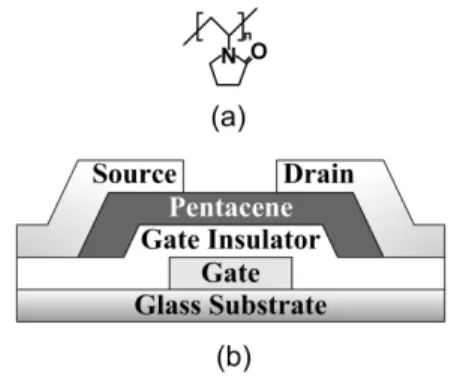
Fig. 1 (a) Molecular structure of PVPy and (b) the cross-section of fabricated the top-contact OTFT.
Electrical Characteristics of Pentacene Thin-Film
Transistors with Polyvinylpyrrolidone Gate Insulator
Dong Wook Kim, Jong Won Lee, Jung Chul Noh, and Jong Sun Choi *
Dept. of Electrical, Information & Control Eng., Hongik Univ., Seoul, Korea Phone: +82-2-320-1488, E-mail: [email protected]
P1-18 / D. W. Kim
• IMID 2009 DIGEST
deposited at a rate of 1.0 Å/s. And 400-Å-thick source and drain electrodes on top of pentacene were thermally evaporated through the third shadow mask with a channel length (L) of 90 μm and width (W) of 300 μm. All evaporation processes were carried out under a base pressure of about 1.6×10⁻⁶ Torr. Figure 1
shows the molecular structure of PVPy and a schematic diagram of the fabricated OTFT.
The crystallinity of each layer was studied by XRD (DMAX 2500, Rigaku) with monochromatic Cu Kα (λ = 1.54 Å) and the surface morphology of pentacene film was examined under AFM (XE-150, PSIA Inc.) using the contact mode. Dielectric property of PVPy and electrical characteristics of OTFTs were measured with impedance analyzer (HP 4192LF, Agilent Technologies) and semiconductor analyzer (EL 421C, Elecs Co.), respectively.
3. Results and discussion
The device for capacitance measurement consists of PVPy layer sandwiched between Al and Au electrodes and the dielectric constant was calculated by the equation (1) [11],
A
d
C
=
ε
0ε
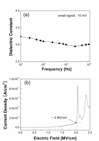
r (1)where C is the measured capacitance, ε0 is the permittivity of free space, εr is the relative dielectric constant of an insulator, A is the area of the capacitor, and d is the insulator thickness. Figure 2 (a) shows the dielectric constants as a function of the applied frequency. The dielectric constant of PVPy was about 3 at 100 kHz, which is in the range of conventional polymeric insulators, such as polystyrene, poly(vinyl acetate), etc. Insulating property of the PVPy gate insulator was also examined using the Al electrode/PVPy (3500Å)/Al electrode structure as shown in Fig. 2 (b). The fabricated PVPy film exhibits the electric field strength of about 2 MV/cm.
The structural and morphological characteristics of pentacene film deposited onto the PVPy layer are shown in Fig. 3. The XRD spectrum shows two diffraction peaks at 5.76° and 6.14° corresponding to thin film phase and triclinic bulk phase, respectively. The strongest peak near 5.76° indicates that the major component of this film is a thin film phase with an interplanar spacing of 15.3 Å, while the diffraction peak near 6.14° corresponds to the bulk phase with an interplanar spacing of 14.4 Å. Considering the length of pentacene molecule to be about 16.5 Å, we found
Fig. 2 (a) Calculated dielectric constants of PVPy at various frquencies and (b) current leakage for 3500-Å-thick PVPy insulator as a function of electric field.
Fig. 3 (a) XRD pattern of 1200-Å-thick pentacene film on the PVPy gate insulator. The inset shows the surface of 300-Å-thick pentacene film deposited on the PVPy gate insulator characterized by AFM (3 μm×3 μm).
P1-18 / D. W. Kim
IMID 2009 DIGEST • that the pentacene molecules are highly ordered in
perpendicular direction to the PVPy layer. Obviously, AFM image shows that pentacene molecules tend to form well-ordered crystallites in herringbone structure as shown in the inset of Fig. 3, where the grain size is measured to be 600-800 nm. Since the interaction of π-electron systems between adjacent molecules depends strongly on their stacking nature, it is expected that vertical alignment of pentacene molecules to the PVPy-coated substrate can provide a strong π-orbital overlap and increase the charge transport properties.
Figure 4 (a) shows the drain current (ID) versus drain voltage (VD) curves of OTFT with the PVPy gate insulator with different negative gate voltages (VG). It is observed that the device exhibited a good saturation behavior and current enhancement was clearly modulated by gate voltages. The corresponding plot of |ID|1/2 versus VG obtained at VD of −30 V is shown in Fig. 4 (b). The field-effect mobility (μeff) was calculated in the saturation region using the equation (2) [12],
2
)
(
2
G T i eff DV
V
L
C
W
I
=
μ
−
(2)where Ci is the capacitance of the gate insulator per unit area, and VT is the threshold voltage. The calculated field-effect mobility and the extracted threshold voltage were 0.23 cm2/Vs and −12.7 V,
respectively. And the on/off current ratio was observed to be about 5×10⁴ with a subthreshold slope
of 3.2 V/decade from the inset of Fig. 4 (b). It is thought that the presented on/off current ratio is relatively low owing to the gate leakage current through the PVPy insulator layer, which is expected to be modified by optimizing the thickness of PVPy layer. Although our TFT with the PVPy gate insulator could not establish an eye-opening progress, yet the reported device performances are decent values as compared with those of devices with polymeric gate insulators. Of particular interest is its stable operation without a shift in the threshold voltage upon a gate voltage sweep direction (see Fig. 4 (b)), because OTFTs adopting polymeric gate insulators often suffer from the threshold voltage shift. Recent work has demonstrated that threshold voltage shift is closely related with charge trapping phenomenon at the interface between organic semiconductors and gate dielectric [13]. Based on the study, we can expect that the PVPy gate insulator formed a defect-free interface and thus contributed to the stable operation with the
Fig. 4 Electrical characteristics of the fabricated OTFT with the PVPy gate insulator: (a) output characteristics with varying VG and (b) transfer curve at VD =
−30 V. The inset in (b) shows Log10|ID|
versus VG plot.
threshold voltage shift less than 0.1 V. This property can make PVPy as a unique candidate for polymeric gate insulator to achieve reliable OTFTs on flexible substrates.
4. Summary
In this study, PVPy was proposed as a new gate insulator for OTFTs. Experimental results showed that PVPy has a dielectric constant of about 3 and the pentacene film deposited onto the PVPy layer tends to form a strong thin film phase with an interplanar spacing of 15.3 Å. The OTFT with the PVPy gate insulator exhibited a field-effect mobility of 0.23 cm2/Vs, a threshold voltage of −12.7 V, and an on/off
current ratio of 5×10⁴ with a subthreshold slope of 3.2 V/decade. In particular, the device showed a stable
P1-18 / D. W. Kim
• IMID 2009 DIGEST
operation without shifts in the threshold voltage upon a gate voltage sweep direction. Within our first hand knowledge, this is the first report studying the characteristics of OTFTs with the PVPy gate insulator. In addition to the presented peculiarities of PVPy, transparency and cross-linkable flexibility also manifest its availability as a gate insulator for high-performance OTFTs. We believe that this study can be helpful for researchers in the field of organic electronics. Further studies are currently in progress towards improving the device performances and developing a cross-linking process below 150°C
Acknowledgement
This research was supported by a grant (F000
4022-2009-32) from Information Display R&D
Center, one of the 21st Century Frontier R&D
Program funded by the Ministry of Knowledge
Economy of Korean Government.
5. References
[1] S.R. Forrest, Nature, 428, 911 (2004).
[2] R. Rotzoll, S. Mohapatra, V. Olariu, R. Wenz, M. Grigas, K. Dimmler, O. Scchekin, and A. Dodabalapur, Appl. Phys. Lett., 88, 123 502 (2006).
[3] L. Wang, D. Fine, S.I. Khondaker, T. Jung, and A. Dodabalapur, Sens. Actuators, B113, 539 (2006). [4] D.R. Hines, V.W. Ballarotto, and E.D. Williams, Y. Shao, S.A. Solin, J. Appl. Phys., 101, 024 503 (2007).
[5] A. Facchetti, M.H. Yoon, and T.J. Marks, Adv. Mater., 17, 1705 (2005).
[6] K.P. Pemstich, S. Haas, D. Oberhoff, C. Goldmann, D.J. Gundlach, B. Batlogg, A.N. Rashid, and G. Schitter, J. Appl. Phys., 96, 6431 (2004).
[7] J.H. Sung, S.J. Park, J.H. Park, H.J. Choi, and J.S. Choi, Synth. Met., 156, 861 (2006).
[8] Z. Bao, A. Dodabalapur, and A.J. Lovinger, Appl. Phys. Lett., 69, 4108 (1996).
[9] W. Xu, H. Chen, H. Li, and M. Wang, Colloids Surf. A, 266, 68 (2005).
[10] J. Swei and J.B. Talbot, J. Appl. Polym. Sci., 90, 1156 (2003).
[11] R.F. Pierret, Field Effect Devices (Addison-Wesley, New Jersey, 1983), p. 45.
[12] S.M. Sze and K.K. NG, Physics of Semiconductor Devices (John Wiley & Sons, New Jersey, 2007), p. 306.
[13] Jiyoul Lee, J. H. Kim, Seongil Im, and D.Y. Jung, J. Appl. Phys., 96, 2301 (2004).