• 검색 결과가 없습니다.

Nanoscale NAND SONOS memory devices including a Seperated double-gate FinFET structure

N/A
N/A
Protected

Academic year: 2021

Share "Nanoscale NAND SONOS memory devices including a Seperated double-gate FinFET structure"

Copied!
7
0
0

로드 중.... (전체 텍스트 보기)

전체 글

(1)

Nanoscale NAND SONOS memory devices including a Seperated double-gate FinFET structure

Hyun-Joo Kim

*

․Kyeong-Rok Kim

**

․Kae-Dal Kwack

* **

*

Dept. of Information Display, Hanyang University, 17 Haengdang-dong, Seongdong-gu, Seoul 133-791, Korea.

**

Dept. of Nanoscale Semiconductor Engineering, Hanyang University, 17 Haengdang-dong, Seongdong-gu, Seoul 133-791, Korea.

Abstract

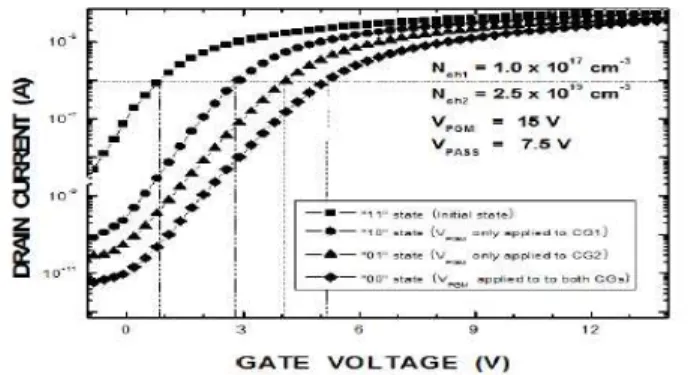
NAND-type SONOS with a separated double-gate FinFET structure (SDF-Fin SONOS) flash memory devices are proposed to reduce the unit cell size of the memory device and increase the memory density in comparison with conventional non volatile memory devices. The proposed memory device consists of a pair of control gates separated along the direction of the Fin width. There are two unique alternative technologies in this study. One is a channel doping method and the other is an oxide thickness variation method, which are used to operate the SDF-Fin SONOS memory device as two-bit.

The fabrication processes and the device characteristics are simulated by using technology comuter-adided(TCAD). The simulation results indicate that the charge trap probability depends on the different channel doping concentration and the tunneling oxide thickness. The proposed SDG-Fin SONOS memory devices hold promise for potential application.

Key word : NAND-type SONOS, SDF-Fin SONOS, Memory devices, Oxide thickness variation method, TCAD

논문접수일 : 2009년 11월 19일 논문수정일 : 2009년 12월 14일 게재확정일 : 2010년 01월 08일

(2)

1. INTRODUCTION

High-density nonvolatile memory (NVM) devices have been of particular interest in devices utilizing flash memories for data storage Hofmann et al(2005), Gupta(2007), Park et al(2006), Kim and Lee(2006). In particular, NAND-type NVMs with nanoscale gates have attracted a great deal of interest owing to their potential application in the NVM devices with ultrahigh-density and low-power elements Sung et al(2006), Lee et al(2004). However, the electrical characteristics of scaled-down conventional NVM devices have delicate problems due to the short channel effect (SCE), the tunneling effect or the leakage current at the oxide/silicon interface, and the coupling capacitance between the cells Kim et al(2007). Fin field-effect transistor (FinFET) structures have emerged as excellent candidates for applications in next-generation NVM devices because of their good SCE immunity, high current drivability, and high punch-through margin Sung et al(2006), Liu et al(2004), Ieong et al(2002). In addition, NVM devices with a double-gate (DG) structure have been studied to overcome SCE and to increase the memory density Cho et al(2006). Because the DG structure utilizes a very thin body to eliminate sub-surface leakage paths between the source and drain, SCE controllability is improved Cho et al(2006).

This paper reports the novel design of nanoscale NAND-type SONOS with a separated double gate FinFET structure (SDG-Fin SONOS). The proposed SDG-Fin SONOS flash memory devices are combined with advantages of the DG FinFET structure and that of the SONOS flash memory device. The 3-D fabrication processes and electrical characteristics for the optimized SDG-Fin SONOS flash memory devices are simulated by using technology computer-aided design (TCAD) tools.

2. PROPOSED STRUCTURES

The proposed SDG-Fin SONOS memory devices are combined with the SONOS memory device and the DG FinFET structure to overcome scaling limits of conventional NVM devices. Fig.1 shows the proposed SDG-Fin SONOS flash memory device with different channel doping concentrations. Because of sharing a source and drain, the total size of the unit string for the NAND flash memory cell array is significantly decreased.

Unique alternative technologies in this study: a channel doping method is used to

operate the SDG-Fin SONOS devices as two-bit. Because the charge trap probability is

dependent on the different channel doping concentrations the optimized SDG-Fin SONOS

memory devices are independently operated as two-bit which resulted in a significant

(3)

increase in the storage density of the NVM devices in comparison with conventional single bit memories. Therefore, the proposed devices significantly increased the scaling down capability and the charge storage density of the NVM devices.

<Fig. 1> Schematic diagram of the proposed SONOS memory devices:

SDG-Fin SONOS flash memory device with different channel doping concentrations

3. DEVICE SIMULATION RESULTS AND DISCUSSION

3.1. Program and erase characteristics

The proposed SONOS flash memory devices are programmed and erased through F-N

tunneling process between the Si-Fin channel and the nitride trap layer. The charges

are trapped into the nitride charge trap layer under the program condition, and

discharged under the erase condition. Fig. 2 shows drain currents as functions of the

gate voltage at the initial state, programmed state, and erased state with each bias

condition, while the N

ch1

and N

ch2

are fixed as 1.0 × 10

17

cm

-3

and 2.5 × 10

19

cm

-3

,

respectively. The V

th

of the initial state, erased state, and programmed state is

approximately 0.8 V, 1.1 V, and 4.1 V, respectively, as shown in Fig.2. This V

th

-shift is

caused by quantities of trapped charges which are varied depending on the initial, erase,

and program condition. Furthermore, the V

th

value of the erased state is almost same as

that of the initial state, so that the V

th

distribution is considered as almost-constant.

(4)

<Fig. 2> Drain currents as functions of the gate voltage at the initial state, programmed state, and erased state with each bias condition, while the N

ch1

and N

ch2

are

fixed as 1.0 × 10

17

cm

-3

and 2.5 × 10

19

cm

-3

, respectively

3.2. Characteristics of different channel doping concentrations

<Fig. 3> Id-Vg characteristics for the SONOS flash memory devices with a SDG FinFET structure before and after program as functions of N

ch2

which is varied from

9.5 × 10

18

cm

-3

to 4.5 × 10

19

cm

-3

, while the N

ch1

is fixed as 1.0 × 10

17

cm

-3

.

Fig.3 compares Id-Vg characteristics for the SONOS flash memory devices with a SDG

FinFET structure before and after program as functions of N

ch2

which is varied from

9.5 × 10

18

cm

-3

to 4.5 × 10

19

cm

-3

, while the N

ch1

is fixed as 1.0 × 10

17

cm

-3

. As N

ch

is

increased, the on current and off-current are decrease in the case of both initial and

programmed state, as shown in Fig.3.

(5)

3.3. Optimized conditions and two-bit operation

Fig. 4 shows the trap charge densities as functions of the programming time for the optimized SDG-Fin SONOS memory device with different channel doping concentrations.

Optimized channel doping condition is obtained as N

ch1

= 1.0 × 10

17

cm

-3

and N

ch2

= 2.5 × 10

19

cm

-3

to divide optimum states. Four independent states divided according to the magnitude of trap charges, as shown in Fig. 4.

<Fig. 4> Trap charge densities as functions of the programming time for the optimized SDG-Fin SONOS memory device with different channel doping concentrations

Fig. 5 shows drain currents for the SDG-Fin SONOS memory device with different channel doping concentrations under the optimized programming conditions. The Vth values of the “11” state, “10” state, “01” state, and “00” state are about 0.8 V, 2.8 V, 4.1 V, and 5.2V, respectively, as shown in Fig.5. The Vth-shift is obtained from the each condition of four states, and is dependent on the channel doping concentrations. The values between the Vth of each state can be defined as the read voltage (VREAD) in the case of sensing operations.

Fig. 5 Drain currents for the SDG-Fin SONOS memory device with different channel

doping concentrations under the optimized programming condition

(6)

4. CONCLUSION

NAND-type SONOS flash memory devices with a SDG FinFET structure are designed to reduce the unit cell size of the memory devices and increase the memory density in comparison with conventional NVM devices. The proposed SDG-Fin SONOS memory devices are combined with the SONOS memory device and the DG FinFET structure to overcome scaling limits of conventional NVM devices. SDG-Fin SONOS memory device with different channel doping concentrations is proposed. The optimized Nch1 and Nch2 are 1.0 × 1017 cm-3 and 2.5 × 1019 cm-3, respectively. The channel doping concentration related to the CG1 sides is different from that of the CG2 side, the charges of the CG1 and CG2 sides trapped through F-N tunneling process are different at the same program voltage conditions. The simulation results of the program/erase characteristics and charge densities indicate that the charge trap probability is dependent on the different channel doping concentrations, so that the optimized SDG-Fin SONOS memory devices are independently operated as two-bit. Therefore, the proposed devices significantly increased the scaling down capability and the charge storage density of the NVM devices.

REFERENCES

[1] F. Hofmann et al(2005), “NVM based on FinFET device structures” Solid-State Electron. 49, 1799.

[2] N. Gupta(2007), “Threshold voltage modeling and gate oxide thickness effect on polycrystalline silicon thin-film transistors” Physica Scripta 76, 628.

[3] B. G. Park et al(2006), “Novel Device Structures for Charge Trap Flash Memories” IEEE Solid-State and Integrated Circuit Technology, ICSICT '06.

[4] K. H. Kim and H. J. Lee(2006), “Novel Structures for a 2-Bit per Cell of Nonvolatile Memory Using an Asymmetric Double Gate” IEICE Trans. Electron. E89-C, 578.

[5] J. Lee et al(2002), “High-Performance 1-Gb NAND Flash Memory With 0.12-μm Technology”

IEEE J. Solid-St. Circ. 37, 1502.

[6] T. Tanaka et al(1994), “A Quick Intelligent Page-Programming Architecture and a Shielded Bitline Sensing Method for 3 V-Only NAND Flash Memory” J. Solid-St. Circ. 29, 1366.

[7] K. Takeuchi et al(1998), “A Multipage Cell Architecture for High-Speed Programming Multilevel NAND Flash Memories” J. Solid-St. Circ. 33, 1228.

[8] J. Lee et al(2003), “A 90-nm CMOS 1.8-V 2-Gb NAND Flash Memory for Mass Storage

(7)

Applications” J. Solid-St Circ. 38, 1934.

[9] S. K. Sung et al(2006), “Fully Integrated SONOS Flash Memory Cell Array With BT (Body Tied)-FinFET Structure” IEEE Trans. Nanotechnol. 5, 174.

[10] Y. K. Lee et al(2004), “Twin SONOS Memory With 30-nm Storage Nodes Under a Merged Gate Fabricated With Inverted Sidewall and Damascene Process” IEEE Electr. Device Lett. 25, 317.

[11] H. G. Kim et al(2007), “Device optimization of the FinFET having an isolated n+/p+ strapped gate” Microelectron. Eng. 84, 1656 (2007).

[12] Y. Liu et al(2004), “A highly threshold Voltage-controllable 4T FinFET with an 8.5-nm-thick Si-fin channel” IEEE Electr. Device Lett. 25, 510.

[13] M. Ieong et al(2002), “ High Performance Double-Gate Device Technology Challenges and Opportunities” IEEE Computer Society, ISQED’02.

[14] S. J. Cho et al(2006), “Design and Optimization of Two-Bit Double-Gate Nonvolatile Memory

Cell for Highly Reliable Operation” IEEE Trans. Nanotechnol. 5, 180.

수치

Fig. 5 shows drain currents for the SDG-Fin SONOS memory device with different channel doping concentrations under the optimized programming conditions

참조

관련 문서