Characteristics Analysis Related with Structure and Size of SONOS Flash Memory Device
Seung-Dong Yang1, Jae-Sub Oh2, Jeong-Gyu Park1, Kwang-Seok Jeong1, Yu-Mi Kim1, Ho-Jin Yun1, Deuk-Sung Choi3, Hee-Deok Lee1, and Ga-Won Lee1,a
1 Department of Electronics Engineering, Chungnam National University, Daejeon 305-764, Korea
2 Nano Patterning Process Team, National Nanofab Center, Daejeon 305-806, Korea
3 Division of Electronics and Information Engineering, Yeungnam College of Science and Technology, Daegu, 705-703 Korea
(Received July 22, 2010; Accepted August 19, 2010)
Abstract: In this paper, Fin-type silicon-oxide-nitride-oxide-silicon (SONOS) flash memory are fabricated and the electrical characteristics are analyzed. Compared to the planar-type SONOS devices, Fin-type SONOS devices show good short channel effect (SCE) immunity due to the enhanced gate controllability. In memory characteristics such as program/erase speed, endurance and data retention, Fin-type SONOS flash memory are also superior to those of conventional planar-type. In addition, Fin-type SONOS device shows improved SCE immunity in accordance with the decrease of Fin width. This is known to be due to the fully depleted mode operation as the Fin width decreases. In Fin-type, however, the memory characteristic improvement is not shown in narrower Fin width. This is thought to be caused by the Fin structure where the electric field of Fin top can interference with the Fin side electric field and be lowered.
Keywords: SONOS, Flash memory, P/E speed, Data retention, Endurance
1. 서 론1)
최근 반도체 소자의 크기가 나노크기로 축소화됨에 따라, 기존 평판채널 MOS 소자의 전기적 특성 제어 가 매우 어려워지고 있는데 [1], 플래시 메모리 분야 에서도 동일한 문제점을 안고 있다. 특히 플래시 메 모리로 현재 가장 많이 사용되고 있는 부유 게이트 구조는 소자가 축소화 되면서 터널 산화막의 두께가 얇아져 전하 누설에 의한 소자 신뢰성에 문제를 일으 a. Corresponding author; [email protected]
키게 된다 [2]. 이를 해결하기 위해 새로운 개념의 메 모리 소자 연구 개발이 활발히 진행되고 있으며, 그 중 SONOS (silicon-oxide-nitride-oxide-silicon) 구조 의 소자가 가장 각광을 받고 있다 [3]. 특히 축소된 SONOS 구조의 플래시 메모리에서 저장 용량의 증가 및 성능 개선을 위해 채널을 3차원으로 제어하는 연 구도 이루어지고 있는데 [4], 그림 1과 같은 Fin-type 구조의 경우가 대표적인 예라 할 수 있다.
본 논문에서는 Fin-type SONOS와 planar-type SONOS 메모리를 제작한 후 전기적 특성을 비교하고,
Fig. 1. 3D-shape of the Fin-type SONOS flash memory structure.
Fin-type SONOS flash memory에서 Lgate와 WFin를 축소 시켜가면서 비교 분석하여 planar-type SONOS 플래시 메모리의 성공적인 비례 축소 가능성을 고찰 하고자 한다.
2. 실험 방법
Fin-type 플래시 메모리 소자 제작을 위하여 p-type (100) 웨이퍼 표면을 Fin 모양으로 식각한 뒤 HDP (high density plasma)로 SiO2를 증착하고 CMP (chemical mechanical planarization)를 하였다. 이후 wet each를 진행하고 tunnel oxide/trapping layer/
control oxide를 3/8/6 nm로 순서대로 증착하였다.
Trapping layer는 silicon nitride를 사용하였다. 이후 gate patterning과 S/D implantation 및 activation을 진행 하였다. 또한 소자 크기별 특성 분석을 위해 Lgate와 WFin를 각각 0.20 ㎛∼0.35 ㎛와 0.18 ㎛∼0.25
㎛로 제작하였다. Planar-type 플래시 메모리는 p-type (100)웨이퍼 위에 터널 oxide를 3 nm키우고, silicon nitride와 control oxide를 각각 8 nm/10 nm 증착했다.
메모리 소자의 특성 평가를 위해 프로그램/소거 방 법은 Fowler-Nordheim (FN) 방식을 이용하였고 전 압 조건은 VG-VT/VD/Vs=7,10/0/0 V로 하였다.
또한, 실온에서 각각의 trapping layer에 대해 endurance, retention 특성을 관찰하였다. Endurance의 경우 1000 cycle 까지 관찰하였고, retention의 경우 문턱전압 변 화가 가장 큰 3시간 동안의 경향성을 관찰하였다. 본 실험에서 사용된 장비는 Hewlett-Packard 사의 Semiconductor Parameter Analyzer (4155B) 와 Pulse Generator Expander (41501B)이다.
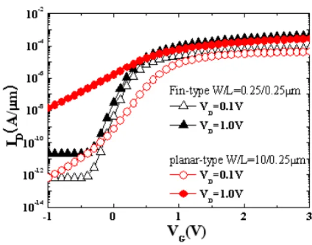
Fig. 2. ID-VG curve of the fabricated Fin-type and planar- type flash memory whose channel lengths are the same with 0.25 um.
Table 1. Extracted electrical parameters of planar/Fin-type devices.
VTH.EXT(V) Ion/off ratio
Slope
(V/dec) Gm.max(S)
FinFET 0.373 1.80E+7 0.095 9.66E-6
Planar 0.672 1.66E+4 0.19 2.99E-4
3. 결과 및 고찰
그림 2는 제작된 Fin과 planar-type 소자의 I-V 특 성 곡선이며 이로부터 전기적 특성 파라미터를 추출 하여 표 1에 정리하였다. VTH.EXT는 Gm.max값에서 IDS 곡선에 접선을 그어 VGS축 절편을 구한 후, VDD/2를 뺀 것이고, Ion/off current ratio는 VGS가 0V 일 때의 ID와 VGS가 1V일 때의 ID의 비율이며, slope 은 subthreshold영역에서 ID-VG 기울기의 역수이다.
그리고 Gm.max는 ID와 VG의 비례상수이다. 이상의 추출된 결과로부터 Fin-type의 경우 planar-type보다 DIBL (drain induced barrier lowering)이 현저히 낮 은 것을 알 수 있다. 또한 subthreshold slope (SS) 및 Ion/Ioff ratio 특성도 매우 우수하다. Fin 구조의 이러한 특성은 기존에 발표된 3차원 구조의 MOSFET 특성들과 일치하며 [5], SCE (short channel effect) immunity 및 전기적 특성 향상은 gate voltage 제어 능력 및 effective width 증가에 기인하는 것으로 판 단된다.
Fig. 3. ID-VG curve of Fin-type SONOS devices according to channel length with fin width fixed. (Lgate=0.20, 0.35 ㎛, WFin=0.25 ㎛)
Fig. 4. ID-VG curve of Fin-type SONOS according to Fin width with channel length fixed. (WFin=0.18, 0.25 ㎛, Lgate
=0.20 ㎛)
그림 3은 Fin-type SONOS flash memory에서 채 널 length에 따른 ID-VG 특성 곡선으로 length가 줄 어들면 평판 구조와 마찬가지로 SCE에 의한 DIBL이 커지면서 VTH 가 감소되는 경향을 보인다 [6].
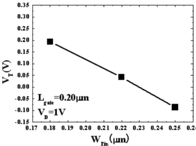
그림 4는 Fin의 width를 줄였을 때 나타나는 ID-VG curve이다. Fin width에 따른 VTH의 변화만을 추출해보면 그림 5와 같다. 두 그림에서 채널 length 가 일정할 때 width 감소에 따라 DIBL이 감소되면서 VTH가 올라가는 것을 알 수 있다. 이는 Fin의 width 가 작아짐에 따라 측벽에 형성되는 inversion layer 하부 영역이 fully depletion되면서 SCE가 개선되는
Fig. 5. VTH versus Fin width for given Lgate of 0.20 um.
Fig. 6. Comparison of P/E speed characteristics of planar vs. Fin-type SONOS devices.
경향을 그대로 보여준다. 따라서 소자의 크기를 감소 시키는 데 있어서 Fin 구조가 매우 효과적임을 확인 할 수 있다.
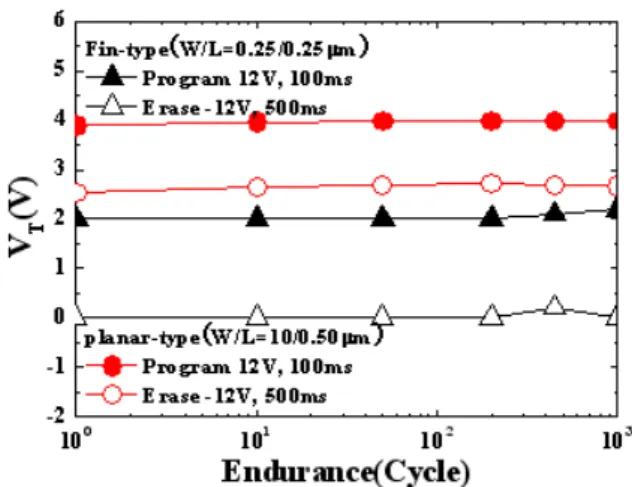
제작된 소자의 메모리 특성 분석과 관련하여 먼저 planar 구조와 축소된 Fin-type 구조의 특성을 비교 하였다. 측정에 사용된 소자의 크기는 planar의 경우 W/L=10/0.50 ㎛ 이며 Fin의 경우 W/L=0.25/0.25 ㎛ 이다. 그림 6은 planar와 Fin-type SONOS 메모리의 프로그램/소거 속도 측정 결과이다. 그림에서와 같이 소자가 축소되었음에도 불구하고, Fin 구조를 도입함 으로써 유사한 프로그램/소거 속도 특성을 확보할 수 있음을 알 수 있다. 그림 7은 planar와 Fin-type SONOS 의 1000 cycle 동안의 Endurance 특성 결과이다.
Fin-type의 경우 planar-type보다 memory window가
Fig. 7. Comparison of endurance characteristics for planar- type vs. Fin-type.
Fig. 8. Comparison of retention characteristics for planar vs. Fin-type SONOS devices.
다소 큰 상황이지만, 1000cycle까지 memory window narrowing이 보이지 않았다. 이것은 Fin 구조에서도 1×10⁵회 프로그램/소거 이후 거의 터널 산화막의 열 화가 없다는 것을 의미한다. 그림 8은 planar-type SONOS 메모리와 Fin-type SONOS 메모리의 기억유 지특성 (data retention)을 나타낸다. 측정 결과 두 소 자에서 대체적으로 비슷한 기억유지특성을 보였지만, Fin-type의 gate 길이가 짧다는 것을 감안하면 개선 된 특성이라고 할 수 있다.
다음으로 Fin 구조에서 채널 length와 Fin width에 대한 메모리 특성을 비교하였다. 그림 9는 Fin-type SONOS flash memory에서 gate length를 줄였을 때 프로그램/소거 속도 특성 결과이다. 그림에서 보면
Fig. 9. Comparison of P/E speed characteristics according to channel length (Lgate=0.20 ㎛, 0.35 ㎛). Here fin width is fixed (WFin=0.25 ㎛).
Fig. 10. Comparison of P/E speed characteristics according to Fin width(WFin.=0.18 ㎛, 0.25 ㎛) Here channel length is fixed (Lgate=0.20 ㎛).
gate length가 0.35 ㎛에서 0.20 ㎛로 축소화 되었을 때 SCE에 의한 영향으로 프로그램/소거 특성이 좋지 않 게 나타난다. 이에 비해 그림 10의 Fin width를 줄였 을 때 프로그램/소거 특성 결과에서는 소자들의 프로 그램/소거 속도 특성이 유사하게 관찰되고 있다. Fin width가 0.18 ㎛로 감소하였을 때 앞의 ID-VG 특성곡 선에서 확인한 바와 같이 SCE가 개선이 되었지만 프 로그램/소거 속도 특성에서는 개선이 나타나지 않는 다. 이는 채널 length 의존성과는 다른 결과로 다음과 같이 해석할 수 있다. 즉 Fin 구조에서 fin width가 축소됨에 따라 fin 측벽의 electric field와 상부의 field가
Fig. 11. Potential contours at a reverse bias of 15 V for TMBS rectifiers with different Fin(mesa) width [7].
상호 간섭을 하게 되면서 상부의 electric field가 감소 하고 이로 인해 동일 bias 조건에서 program/erase가 불리해 질 수 있다. Fin 구조에서의 potential 분포와 관련하여 유사한 연구결과가 TMBS (trench mos barrier schottky) rectifier 구조에서 발표된 바 있는 데 그림 11은 Fin(Mesa)구조에서 Fin width에 따른 electric field의 분포로 width가 감소함에 따라 상부 의 electric field가 감소하는 것을 simulation한 결과 이다 [7].
4. 결 론
본 논문에서는 Fin-type SONOS 플래쉬 메모리의 비례 축소 가능성을 고찰하기 위해 Fin-type과 planar- type의 SONOS 메모리를 제작하고, 단위소자 및 메 모리의 전기적 특성을 비교 분석하였다. Fin-type 소 자의 경우 planar 소자에 비하여 SCE에 의한 소자 특성 열화가 개선되면서 DIBL이 현저히 낮아짐을 확 인하였다. 더욱이 sub-threshold slope 및 구동전류 (on current)도 우수하였으며, 특히 메모리 특성의 경우 우수한 SCE immunity로 인해 P/E speed 및 data retention 특성의 열화를 보이지 않음을 알 수 있었 다. 본 연구에서는 또한 Fin-type SONOS 메모리의 gate length 및 fin width에 의한 소자 특성을 비교
감사의 글
이 논문은 2009년도 정부 (교육과학기술부)의 재원 으로 한국연구재단의 지원을 받아 수행된 기초연구사 업 (No. 2009-0068143) 및 지식경제부와 한국산업 기 술재단의 전략기술 인력양성사업으로 수행된 연구결 과임.
REFERENCES
[1] L. Chang, Y.-K. Choi, D. Ha, P. Ranade, S. Xiong, J.
Bokor, C. Hu, and T. J. King, Proc. IEEE, 91, 1860 (2003).
[2] International Technology Roadmap for Semiconductors (ITRS) 2001 Edition, Table 38a, 38b (2001).
[3] C. W. Kim, M. K. Kim, and J. W. Lee, Physics and High Technology 13, 2 (2004).
[4] S. Tiwari, F. Rana, H. Hanafi, A. Hartstein, E. F. Crabbé, and K. Chan, Appl. Phys. Lett. 68, 1377 (1996).
[5] T. Park, S. Choi, D. H. Lee, J. R. Yoo, B. C. Lee, J. Y.
Kim, C. G. Lee, K. K. Chi, S. H. Hong, S. J. Hynn, Y. G. Shin, J. N. Han, I. S. Park, U. J. Chung, J. T.
Moon, E. Yoon, and J. H. Lee, Symp. VLSI Technol.
Dig. Tech. Papers (IEEE, 2003) p. 135
[6] F. Daugé, J. Pretet, S. Cristoloveanu, A. Vandooren, L. Mathew, J. Jomaah, and B. -Y. Nguyen, Solid- State Electron. 48, 535 (2004).
[7] M. Mehrotra and B. J. Baliga, IEDM '93 Tech. Dig.
(IEEE, Washington DC, USA, 1993) p. 675.
![Fig. 11. Potential contours at a reverse bias of 15 V for TMBS rectifiers with different Fin(mesa) width [7].](https://thumb-ap.123doks.com/thumbv2/123dokinfo/5571262.478091/5.892.101.421.190.405/fig-potential-contours-reverse-tmbs-rectifiers-different-width.webp)
