반도체디스플레이기술학회지 제18권 제4호(2019년 12월)
Journal of the Semiconductor & Display Technology, Vol. 18, No. 4. December 2019.
SONOS NAND 플래시 메모리 소자에서의 Lateral Charge Migration에 의한 소자 안정성 연구
성재영*· 정준교*· 이가원*†
*†충남대학교 전자공학과
Reliability Analysis by Lateral Charge Migration in Charge Trapping Layer of SONOS NAND Flash Memory Devices
Jae Young Sung*, Jun Kyo Jeong* and Ga Won Lee*†
*†Department of Electronics Engineering, Chungnam National University
ABSTRACT
As the NAND flash memory goes to 3D vertical Silicon-Oxide-Nitride-Oxide-Silicon (SONOS) structure, the lateral charge migration can be critical in the reliability performance. Even more, with miniaturization of flash memory cell device, just a little movement of trapped charge can cause reliability problems. In this paper, we propose a method of predicting the trapped charge profile in the retention mode. Charge diffusivity in the charge trapping layer (Si3N4) was extracted experimentally, and the effect on the trapped charge profile was demonstrated by the simulation and experiment.
Key Words : Flash memory, Lateral charge migration, Diffusivty
1. 서 론1
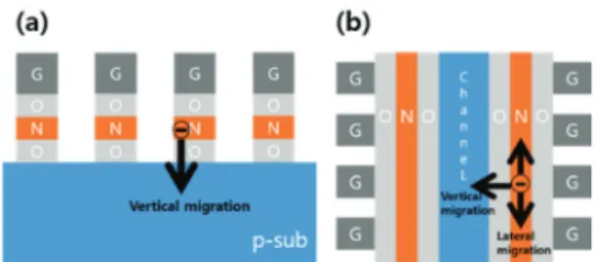
4차산업이 발달함에 따라 cloud 서비스 확대, IoT 및 AI 등 새로운 IT 수요 환경에 대응하기 위해 더 많은 데이터 를 저장할 수 있는 비 휘발성 메모리에 대한 수요가 급속 도로 증가하고 있다. 이에 집적도 향상을 위해 소자의 스 케일링 다운이 지속되었고 최근에는 2D 구조의 한계를 넘기 위해 채널을 수직으로 형성시킨 3D Silicon-Oxide- Nitride-Oxide-Silicon (SONOS) 구조의 NAND 플래시 메모리 가 등장하였다. 3D 구조의 메모리는 2D 구조를 사용할 때 보다 집적도 측면에서 급격한 향상을 보였지만 구조상의 차이로 인해 신뢰성 부분에서 이전에는 고려하지 않아도 되었던 새로운 문제가 발생되었다 [1] [2]. Fig. 1은 3D SONOS NAND 플래시 메모리 구조에서 charge trapping layer(CTL)인 nitride에 저장되어 있는 전하가 이동할 수 있
†E-mail: [email protected]
Fig. 1. Schematic diagram of charge loss possible in NAND flash memory: (a) Vertical charge migration in the 2D structure and (b) vertical and lateral charge migration in the 3D structure.
는 경로를 보여준다.
Fig. 1(a)의 기존 2D 구조에서는 각 셀의 CTL이 분리되 어 있기 때문에 tunneling oxide나 blocking oxide를 경유한 vertical charge migration만 발생한다 [3]. 하지만 Fig. 1(b)의 3D 구조에서는 하나의 스트링을 구성하는 여러 셀들이 CTL 을 공유하고 있는 구조이기 때문에 이웃 셀 방향으로의
SONOS NAND 플래시 메모리 소자에서의 Lateral Charge Migration 에 의한 소자 안정성 연구 139
lateral charge migration이 추가적으로 발생할 수 있다 [4][5].
3D소자의 소형화로 셀 간 거리가 계속 줄어듦에 따라 lateral charge migration으로 인한 인접 셀의 영향은 점점 커 지므로 메모리 동작의 신뢰성 문제를 심화시킬 수 있다 [6]. 플래시 메모리의 신뢰성을 나타내는 지표로는 data retention, program/erase endurance, noise 등이 있다. 그 중 data retention 특성은 메모리에 데이터를 저장하고 얼마나 오랫 동안 데이터 손실 없이 유지할 수 있는지를 나타내는 중 요한 지표이다. 따라서 lateral charge migration의 정도를 예측 하고 이로 인한 data retention 특성 열화를 정량적으로 평 가할 수 있다면 3D 메모리 신뢰성 개선에 매우 유용할 것이다.
본 연구에서는 SONOS구조의 mesh-type capacitor를 제작 하고 프로그램 된 상태에서 전하 손실 측정을 통해 lateral charge migration에 대한 diffusivity를 추출하였으며 구해진 diffusivity를 이용해 trapped charge 분포를 시뮬레이션 하였 다. 특히 본 논문에서는 셀 간 space 영역에 축적된 전하 에 의한 소자 안정성 문제를 실험과 시뮬레이션을 통해 확인하고자 하였다. 향후 셀 간 간격이 지속적으로 축소 되는 상황에서 본 논문에서 제시한 바와 같이 lateral charge migration의 정도를 정량적으로 지표화 할 수 있는 diffusivity를 추출할 수 있다면 lateral charge migration에 의한 메모리 성능의 안정성 평가가 효율적으로 이루어질 수 있을 것이다.
2. 실험 방법 2.1 소자 제작 공정
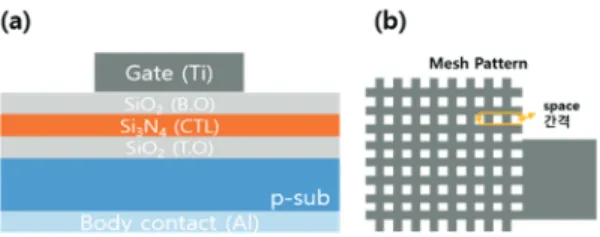
본 실험에서는 tunneling oxide, nitride (CTL), blocking oxide, gate 구조의 SONOS-type capacitor를 제작했다. 기판은 p-type silicon을 사용하였고 tunneling oxide는 7 nm 두께의 SiO2를 dry oxidation으로 형성시켰다. LPCVD공정을 이용해 CTL로 15 nm 두께의 Si3N4와 blocking oxide로 15 nm 두께의 SiO2를 증착했다. RF sputter를 사용해 게이트에 Titanum 100nm를 증 착하고 gate 형성을 위한 lithography와 etch를 진행하였다.
마지막으로 Body전극으로 Aluminum을 100 nm 두께로 증 착시켰다.
2.2 소자 구조
Fig. 2(a)는 제작된 소자의 모식도이다. 게이트 패턴의 경 우 vertical charge migration이 주로 일어나는 기존의 square- type pattern과 함께 lateral charge migration이 일어날 수 있도록 게이트 둘레(perimeter)의 길이를 크게 증가시킨 mesh-type pattern을 함께 사용하였다. Fig. 2(b)는 mesh-type 패터닝을 위 해 사용된 게이트 mask이다. Mesh-type의 경우 lateral charge
migration에 의한 안정성 평가의 최적 조건을 찾기 위해 space 간격을 달리하는 소자들을 제작하였다.
Fig. 2. Schematic of SONOS-type capacitor: (a) cross section of the device and (b) top view of mask used for the mesh-type gate patterning. Here, the space is varied to extract the optimal distance for the evaluation of the lateral charge migration.
2.3 Diffusivity 추출 방법
Perimeter 비율이 큰 mesh-type pattern 소자와 동일 면적의 square-type pattern에 동일한 프로그램 전압을 가한 후 retention mode에서 flat band voltage (VFB)를 시간에 따라 측정 하였다. Program과 erase는 Hewlett Packard 41501A pulse generator를 사용하였고 VFB는 Hewlett Packard 4284A precision LCR meter를 이용해 C-V 곡선을 측정하여 추출하였다.
이러한 조건 하에서 시간에 따른 VFB shift(ΔVFB)를 설명 할 수 있는 charge distribution으로 아래와 같은 분포식을 사용하였다.
n erf √ erf √ (1)
n0 : initial charge density [C/cm3] W : Gate length [cm]
D : electron diffusivity [cm2/sec]
t : time [sec]
n : charge density [C/cm3]
식 (1)은 Fick’s law[7]에 따른 시간과 공간의 함수로 셀 전하 분포를 표현하기 위해 사용한 식이다. 이 때 n0는 프 로그램 한 직후의 charge density, W는 소자의 gate length, t는 retention 시간, D는 electron diffusivity이며 n은 diffusion이 진행 된 후의 charge density이다. 소자를 제작하고 retention mode에 서의 VFB를 시간에 따라 측정하였으며 이러한 경향과 일 치하는 전하 분포를 설명할 수 있는 D값을 Si3N4 내에서 의 charge (electron) diffusivity로 정하였다.
성재영 · 정준교 · 이가원 140
3. 실험 결과 3.1 Electron diffusivity 추출
Fig. 3. (a) Program/retention measurement at square-type pattern and mesh-type pattern with the same gate area and (b) comparison of ΔVFB over time at two pattern.
Fig. 3은 게이트 면적이 같은 square-type과 mesh-type 소자 를 동일한 조건으로 프로그램 한 뒤 retention mode에서 Δ VFB 를 측정한 결과이다. 면적이 같기 때문에 두 소자에 서의 vertical charge migration 양은 같다고 가정할 수 있다.
따라서 Fig. 3에서 나타나는 ΔVFB양의 차이가 lateral charge migration 양이라고 볼 수 있다.
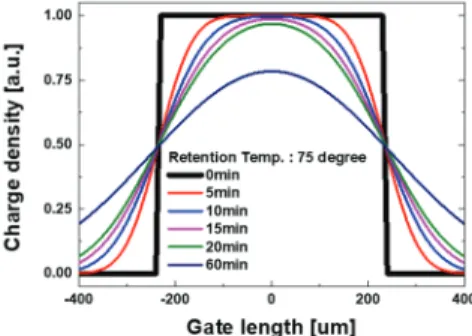
Fig. 4. Simulation results for the charge distribution in CTL considering the lateral charge loss in the retention mode after programming.
이렇게 시간에 대해서 lateral charge migration에의한 전하 손실 양을 추출하게 되면 앞의 식 (1)을 통해 전하의 프로 파일을 구할 수 있게 되는데 결과는 Fig. 4와 같다. Fig. 4에 도시한 프로파일의 경우 전하들의 확산 계수(D) 값으로
~10-9 cm2/s를 얻을 수 있었다. 이렇게 CTL에 트랩된 전하들 의 확산 계수 값을 알 경우 다양한 기하학적, 전기적 조 건 하에서 전하 분포의 변화를 예측할 수 있다.
3.2 Program 상태에서의 space 전하 영향
Fig. 5. (a) Charge distribution just after program and (b) charge distribution after lateral charge migration to space was proceeded.
Fig. 6. Simulation results on the charge profile of the programmed cells and the space between the cells.
The space charge increases according to the number of program cycling. Here, the electron diffusivity is assumed to be 10-9 cm2/s, which is extracted by the experiment.
3D NAND flash 소자에서 하나의 memory string을 구성하 는 셀 간 간섭 현상의 하나로 특정 셀의 데이터 값이 양 쪽에 있는 셀의 프로그램 상태 및 이력에 따라 바뀔 수 있는 현상을 생각해 볼 수 있다. 즉, 3D 구조에서는 셀 간 CTL이 격리되는 2D 구조와는 달리 프로그램 된 셀에 국 부적으로 트랩된 전하가 retention mode에서 셀 간 space로 lateral migration 할 수 있다. 이 경우 space 전하 양은 program 이력에 따라 달라질 수 있으며 이후 주변 셀의 전하 분포 에 영향을 줄 수 있기 때문이다.
셀 간 space 영역에 축적된 전하의 양에 따라 프로그램 된 셀의 트랩 전하 프로파일이 달라질 수 있음을 실험적 으로 확인하기 위해 mesh-type 셀을 program 시킨 후 75℃
에서 1시간동안 ΔVFB 양을 측정하였다. 이를 도시화 한 것이 Fig. 5로 프로그램 시 게이트 영역 아래에 트랩된 전
SONOS NAND 플래시 메모리 소자에서의 Lateral Charge Migration 에 의한 소자 안정성 연구 141
Fig. 7. C-V measurement results in programmed mesh-type device in the retention mode. As the number of program increases, the ΔVFB decreases. Here, the temperature of retention mode is 75℃.
Fig. 8. Extracted ΔVFB, which was saturated and the blue point is the result of the square-type pattern under the same condition.
하가 retention mode에서 space 영역으로 확산해 나감을 보 인다. 앞에서 언급한 바와 같이 lateral charge migration에 대 한 확산 계수를 알고 있을 경우 이러한 실험 조건 하에서 의 셀 전하 프로파일을 예측할 수 있으며 program과 retention을 3회 반복할 때 결과가 Fig. 6이다. 반복 횟수가 증가할수록 space 영역에 더 많은 전하가 쌓이는 것을 확 인할 수 있다. 이렇게 program 과정에 따른 space 전하 양 이 증가하게 되면 space 영역으로의 diffusion이 감소하게 되어 lateral migration에 의한 전하 손실 양이 감소할 것을 예측할 수 있다. 이를 실험적으로 확인한 결과가 Fig. 7이 다. Fig. 8은 program 반복 횟수에 따라 retention mode에서의 ΔVFB 양을 측정한 결과로 횟수가 증가할수록 ΔVFB 양이 감소하면서 saturation 되는 경향을 보인다. ΔVFB가 0으로 수렴하지 않는 이유는 retention mode에서 수직 방향으로의 전하 손실이 함께 발생하기 때문이다. Fig. 8에 수직 방향 으로의 전하 손실만을 가정한 동일 면적의 square-type 소 자의ΔVFB를측정하여 함께 나타내었다. 측정값을 1.582 V 로 mesh-type 소자의 saturation 값인 1.532 V와 유사함을 확 인할 수 있다.
3.3 Erase 상태에서의 space 전하 영향
Fig. 9. Lateral migration of space charges to the adjacent erased cells during retention mode.
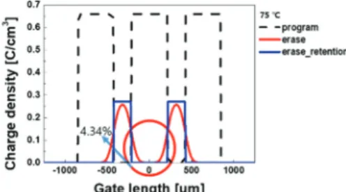
데이터가 소거된 erased cell에서의 space 전하 양에 따른 전기적 특성 평가를 위해 반복적인 program을 통해 셀 간 space 영역에 전하를 축적 시킨 후 erase 동작을 통해 게이 트 영역 아래 전하를 모두 소거시킨 상태에서의 ΔVFB를 측정하였다. 이를 도식화한 것이 Fig. 9이다. 실제 측정을 진행하기 전에 시뮬레이션을 통해 space charge 값을 예상 한 결과는 Fig. 10과 같다. 75℃에서 1시간 후에 program 상 태의 4.34 %만큼의 전하가 셀로 이동하였고 이를 VFB로 환산해보면 약 0.4 V가 증가하게 된다.
Fig. 10. Simulation results on the charge profile of the erased cell, which is affected by the space charges.
Here, the electron diffusivity is assumed to be 10-9 cm2/s, which is extracted by the experiment.
Fig. 11은 제작된 소자에서의 측정 결과로 시뮬레이션과 동일하게 75℃에서 1시간후에 약 0.4V가 증가하는 것을 확인할 수 있다. Retention mode의 온도를 125℃로 증가시켰 을 경우 ΔVFB가 더 크게 증가하였는데 이는 cell space에 축 적된 전하의 diffusivity가 고온에서 증가하기 때문으로 판 단된다. 하지만 150℃의 경우 오히려 ΔVFB가 감소하는 것 으로 나타나는데 이는 임계 온도 이상에서는 수직 방향 의 charge loss가 크게 증가하는 것으로 추측되며 온도 의존 성에 의한 심화 연구는 계속 진행 중이다.
성재영 · 정준교 · 이가원 142
Fig. 11. Measurement results of ΔVFB in erased mesh-type device in the retention mode according to time.
Increase of VFB is caused by the charges in space region. Here, the temperature of retention mode is 75℃.
4. 결 론
본 논문에서는 3D NAND flash 메모리 소자의 신뢰성을 향상시킬 수 있는 방법으로 lateral charge migration의 정량 지표로 electron diffusivity 추출과 이를 기반으로 한 전하 분 포 시뮬레이션 및 실험 결과를 제시하였다. Lateral migration 정도를 평가할 수 있는 mesh-type의 SONOS capacitor를 제작 하고 프로그램한 뒤 retention mode에서의 전하 손실을 분 석하여 charge의 diffusivity를 추출하였고 이를 기반으로 전 하 분포를 도시화하였다. 특히 본 논문에서는 셀 간 space 영역에 축적된 전하에 의해서 프로그램된 셀과 소거된 셀의 전기적 특성이 영향을 받을 수 있음을 실험과 시뮬 레이션을 통해 모두 확인하였다. 향 후 셀 간 간격이 지 속적으로 축소되는 상황에서 lateral migration의 정도를 정 량적으로 지표화할 수 있는diffusivity를 추출하고 이를 기 반으로 메모리 소자의 동작 안정성을 예측하여 소자 개 발이 이루어진다면 더욱 효율적인 제품 생산이 가능할 것으로 기대된다.
감사의 글
이 논문은 2019년도 정부(과학기술정보통신부)의 재원
으로 한국연구재단-나노·소재기술개발사업의 지원을 받 아 수행된 연구임 (2009-0082580). 또한 2019년도 정부(미래 창조과학부)의 재원으로 한국연구재단의 지원을 받아 수 행된 연구임 (NRF-2019R1A2C1084717).
참고문헌
1. A.S. Spinelli, C.M. Compagnoni and A.L. Lacaita,
“Reliability of NAND flash memories : Planar cells and emerging issues in 3D devices”, Computers 6.2, 2017.
2. A. Maconi, A. Arreghini, C.M. Compagnoni, A.S.
Spinelli, J. Van Houdt and A.L. Lacaita, “Comprehensive investigation of the impact of lateral charge migration on retention performance of planar and 3D SONOS devices”, Solid-State Electronics, 2012.
3. E.W. Lim and R. Ismail, “Conduction mechanism of valence change resistive switching memory : a survey”, Electronics, 2015.
4. S. H. Kim, S. D. Yang, J. S. Kim, J. K. Jeong, H. D. Lee and G. W. Lee, “Charge spreading effect of stored charge on retention characteristics in SONOS NAND Flash memory devices”, Transactions on Electrical and Electronic Materials, pp. 1863-186, 2015.
5. C. Woo, S. Kim, J. Park, D. Lee, M. Kang and H. Shin,
“Modeling of lateral migration mechanism during the retention operation in 3D NAND flash memories.” IEEE 2019 Electron Devices Technology and Manufacturing Conference, 2019.
6. A. Grossi, C. Zambelli and P. Olivio, “Reliability of 3D NAND flash memories”, 3D Flash Memories, pp. 29-62, 2016.
7. M. Menard and R.W. Paynter, “Fick’s law of diffusion depth profiles applied to the degradation of oxidized polystyrene during ARXPS analysis”, Surface and Interface Analysis : An International Journal devoted to the development and application of techniques for the analysis of surfaces, interfaces and thin films, 2005.
접수일: 2019년 12월 23일, 심사일: 2019년 12월 26일, 게재확정일: 2019년 12월 27일