한국산업정보학회논문지 제17권 제3호(2012. 6)
The Impact of TDDB Failure on Nanoscale CMOS Digital Circuits
†Yeon-Bo Kim* and Kyung Ki Kim**
Abstract This paper presents the impact of time dependent dielectric breakdown (TDDB, also called as gate oxide breakdown) failure on nanoscale digital CMOS Circuits. Recently, TDDB for ultra-thin gate oxides has been considered as one of the critical reliability issues which can lead to performance degradation or logic failures in nanoscale CMOS devices.
Also, leakage power in the standby mode can be increased significantly. In this paper, TDDB aging effects on large CMOS digital circuits in the 45nm technology are analyzed.
Simulation results show that TDDB effect on MOSFET circuits can result in more significant increase of power consumption compared to delay increase.
Key Words : Reliability, Aging effect, Time dependent dielectric breakdown, TDDB, Gate oxide breakdown
1. Introduction†
As MOSFET technology is scaled down more aggressively, reliability issues have become one of the most important issues in sensor systems and synchronous systems [1][2], especially in the nanoscale MOSFET technology [3]. Under normal operation condi- tions, a transistor device can be affected by various reliability mechanisms (or aging phenomena) such as negative bias temperature instability (NBTI), hot carrier injection (HCI), and time-dependent dielectric breakdown (TDDB). These mechanisms lead to device aging, resulting in performance degradation and eventually design failure during the expected system lifetime [3]-[5].
Recently, the oxide thickness of less than 2nm is
†This research was supported by the Daegu University Research Grant, 2011.
* Professor, Department of Electronic Engineering, Daegu University, South Korea, (e-mail: [email protected])
** Assistant Professor, Department of Electronic Engineering, Daegu University, South Korea, (e-mail: [email protected]:
Corresponding author)
common in state-of-the-art technologies, and TDDB is becoming one of key challenges among these reliability mechanisms [6][7].
TDDB can be translated in gate oxide breakdown failure rate or failure in time (FIT). The lower TDDB is, the higher the failure rate or FIT is. At the current operating voltages of MOSFETs, the most widely accepted degradation model is the “trap creation” process which is attributed to hydrogen release from the anode. Hydrogenous species (either protons or atomic hydrogen) are freed from the silicon layers by energetic electrons and then drift and diffuse through the oxide reacting with the lattice to produce traps and other defects.
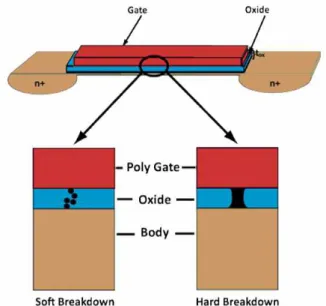
Breakdown begins when traps is formed across the gate oxide. At the beginning of the breakdown, the traps are non-overlapping and thus do not make a conducting path from the gate to the substrate or gate to source and drain. However, as more and more traps are created in the gate-oxide, traps start to form a conducting path as shown in Fig. 1. This type of breakdown is called soft breakdown (SBD).
<Figure 1> NMOSFET cross section illus- trating TDDB.
<Figure 2> Wear-out and breakdown model for thin gate oxides [8].
Once there is a conducting path, new traps are created by thermal damage, which in turn allows for increased conductance. The cycle of conduction leading to increased heat and increased conduction brings about thermal runaway and finally causes a lateral propagation of the breakdown spot. The silicon within the breakdown spot starts to be melted; oxygen is released; and a silicon filament is built in the breakdown spot. This type of breakdown is called hard breakdown (HBD), and the cross section of the gate oxide after hard
breakdown is shown in Fig. 1 [8][9].
Figure 2 shows the variation of leakage path current depending on the wear-out and breakdown phase for thin gate oxides. At the end of the phase I, the traps start to be creased. During Phase II, moving traps lead to random fluctuation in the leakage current, power and delay, where the device is still functional. In phase III, the conduction path is created in the oxide, the leakage current is exponentially increased, then finally the conduction path causes a catastrophic failure of the device [10].
The precise point at which the breakdown occurs is statistically distributed. As a result, only statistical averages can be predicted. TDDB is typically treated statistically using the Weibull distribution [11]. For this reason, usually a large gate oxide area has to be used in order to be able to detect the breakdown. Gate oxide breakdown manifests itself as an increase of gate current while retaining its insulating properties (soft breakdown-SBD or hard breakdown-HBD) that happens when I-V curve becomes linear, i.e., manifests a resistor- like behavior. For thinner gate oxides (≤30 Åm), SBD is the most likely event.
The probability of PMOS gate-oxide breakdown is at least an order less than that of NMOS breakdown [12], hence the TDDB effect only on NMOS devices is considered in this paper.
Recently, many researches on the TDDB effect have been proposed, but they have mainly focused on device physics not circuit- level analysis.
Although a few researches on the circuit-level analysis of TDDB in nano- scale CMOS circuits have been proposed, they have concentrated on mathematical modeling and performance degradations only in simple digital circuits. Therefore, in this paper, TDDB impact on digital circuit is analyzed at a 45nm technology node using inverter chain, and ISCAS85 benchmark circuit. In addition, TDDB impact on various parameters (delay, power, supply variation, process variation, and noise margin) in digital circuits is analyzed.
2. TDDB Modeling
At current operating voltages for MOSFETs, the degradation mechanism can be approximat- ed by an exponential function of voltage applied across gate oxide and Arrhenius function of temperature as follows [6]:
·exp
·exp (1) where Vg is the voltage across gate oxide, Ea is the activation Energy, k is the Boltzman's constant, T is the junction temperature, C and β are the technology specific constants.
Gate oxide breakdown is sensitive to:
∙Voltage across the gate oxide (Vg): The higher Vg and the higher Vg duty cycles the shorter TDDB. For this reason, worst case condition for gate oxide occurs when the device is operated in DC mode (100% duty cycle).
∙Junction temperature
∙Gate oxide thickness: The thinner the gate oxide the more difficult it is to get good quality oxides and interfaces. Nitrided gate oxides have shown improved TDDB compared to SiO2.
∙Gate oxide area: The bigger the gate oxide area the higher the gate oxide breakdown induced failure rate. SRAMs typically have gate oxide area and can be good vehicles to test gate oxide lifetime.
In this paper, for post-breakdown analysis at the circuit-level, a MOSFET with the oxide breakdown is modeled using two breakdown resistors (RBD) as shown in Fig.3 [12]. The RBD value ranges from GΩ (no TDDB) to a few hundreds of KΩ(HBD). The time- dependent gate to source/drain resistor model was experimentally verified in Ref. [13].
<Figure 3> TDDB model for NMOS.
<Table 1> Gate Oxide Stress During Inverter Operation
Vin
state PMOS NMOS
Low
Vg = Vss, Vs = Vdd, Vd = Vdd, Vsub = Vdd Causing HBD
Vg = Vss, Vs = Vss, Vd = Vdd, Vsub = Vss Causing G/S stress
High
Vg = Vdd, Vs = Vdd, Vd = Vss, Vsub = Vdd Causing G/D stress
Vg = Vdd, Vs = Vss, Vd = Vss, Vsub = Vss Causing HBD
The worst stresses for NMOS and PMOS gate oxide take place when NMOS and PMOS are in ON state. Table 1 summarizes inverter states and resultant stress on gate oxide. For this reason, in calculating product gate oxide FIT, we make the assumptions that duty cycle of the voltage across gate oxide is 50%. However, when PMOS and NMOS are off, respectively, gate/drain and gate/source over- laps are stressed, i.e., gate oxide in overlap region is continuously stressed. The FIT contribution from this stress condition is small due to the relatively smaller gate oxide area in the overlap regions.
Based on the TDDB analysis, there is a maximum voltage across gate oxide that a given technology can support, for a given gate oxide area and failure rate. The oxide thickness, for a
<Figure 4> TDDB resistance in nMOS in the inverter
<Figure 5> TDDB effect on the delay of a inverter chain consisting of 110 inverters
technology, is determined so that this voltage is not exceeded, in a dc sense, for any circuit design.
However, when signals are driven, there is a certain amount of overshoot/undershoot in the waveform which can result in accelerated gate oxide wear-out and lower reliability, if appropriate limits are not established.
In Fig. 4, it is assumed that the NMOS (MN1) of the 1st inverter is stressed by the gate oxide breakdown; while Input signal is changed from logic
“0” to “1’, the NMOS of the 1st inverter is turned on; the node n1 capacitor starts to be discharged through MN1, but the discharge time is longer than the normal discharging time because of the
breakdown resistor. As a result, this makes the charging time at Output node longer, which means the propagation time from Input to Output will be longer comparing to the normal case without TDDB. The propagation time depends on the breakdown resistor value: if the resistor is large, the charging time at Output node will be a little increased; however, if the resistor is small, the charging time at Output node will be much more increased due to the small voltage-swing at node n1 caused by the small breakdown resistor.
On the other hand, while Input signal is changed from logic “1” to “0’, the PMOS of the 1st inverter is turned on; the node n1 capacitor starts to be discharged through MN1, but the discharge time is longer than the normal discharging time because of the breakdown resistor. As a result, this makes the charging time at Output node longer, which means the propagation time from Input to Output will be longer comparing to the normal case without TDDB. The propagation time depends on the breakdown resistor value: if the resistor is large, the charging time at Output node will be a little increased; however, if the resistor is small, the charging time at Output node will be much more increased due to the small voltage-swing at node n1 caused by the small breakdown resistor.
Putting the abovementioned two transitions together, if the breakdown resistor is small, the propagation time from Input to Output will be increased; if the breakdown resistor is large, the propagation time from Input to Output will be decreased. This means that the propagation time in the case with SBD might be shorter than the time in the normal case without TDDB; and as a gate oxide goes to HDB, the propagation time might be longer than the time in the normal case without TDDB.
Figure 5 shows TDDB effect on the delay of a inverter chain consisting of 110 inverters, where the TDDB resistors are randomly placed in the inverter chain. The simulation presents that as the TDDB
<Figure 6> TDDB effect on CMOS voltage transfer characteristic.
<Figure 7> TDDB rate dependence of power consumption in different temperature.
<Figure 8> TDDB rate dependence of delay in different temperature.
resistor size decreases, the delay of the inverter chain becomes decreased around up to 45KΩ, then
the delay get increased, and finally the inverter chain goes to a functional failure.
3. TDDB Impact on Digital Circuits
<Figure 9> TDDB rate dependence of power consumption in different process corner.
<Figure 10> TDDB rate dependence of delay in different process corner.
In terms of the voltage transfer characteris- tic of an inverter, the oxide breakdown in the inverter results in an upward and downward shift in the VOL and VOH value, respectively, as illustrated in Fig. 6. When TDDB is generated in the inverter, noise margin will be decreased. Finally, the inverter can be easily affected by noise.
The PVT variation will also change the impact of TDDB on digital circuit. We simulate the inverter chain with different PVT conditions, where the
<Figure 11> TDDB rate dependence of power consumption in different voltage.
<Figure 12> TDDB rate dependence of delay in different voltage.
stressed devices having random resistor values ranging from 100KΩ to 300KΩ at random locations.
The process corner includes a fast corner, a typical corner and a slow corner. The temperature varies from 0°C to 125°C with 25°C as a step. The supply voltage is experienced within ±5% range of typical supply voltage, which is 1V.
From Fig. 8 to Fig. 12 show the TDDB rate dependence of power and delay in different PVT corner, respectively. The simulation results present that the TDDB effect on digital circuits in different PVT corner gets more serious as the TDDB rate goes up.
4. Simulation Results
In order to show the TDDB effect on real digital circuits, various 45nm ISCAS85 benchmark circuits considering the gate oxide breakdown model (breakdown resistor model) have been implemented and evaluated HSPICE, where the stressed devices having random resistor values ranging from 100KΩ to 300KΩ at random locations. Table 2 and 3 presents the delay and power simulation results of ISCAS85 benchmark circuits, respectively. As the percentage of TDDB-stressed devices in the
<Table 2> Delay Variation for ISCAS85 Circuits Considering TDDB Stress
TDDB Rate
(%) C1980
(sec) C3540
(sec) C5315 (sec) 0% 5.25e-10 7.18e-10 6.28e-10 10% 5.40e-10 7.02e-10 6.25e-10 20% 5.45e-10 7.94e-10 6.93e-10 30% 5.94e-10 8.01e-10 7.78e-10 40% 5.29e-10 7.80e-10 6.87e-10 50% 5.28e-10 7.34e-10 6.82e-10 60% 6.01e-10 8.72e-10 7.91e-10 70% 5.97e-10 7.61e-10 8.11e-10 80% 6.72e-10 9.21e-10 8.96e-10
90% 7.37e-10 Fail 9.44e-10
100% 7.90e-10 Fail 9.86e-10
Avg. Rate 6.9% 8.21% 8.86%
<Table 3> Power Variation for ISCAS85 Circuits Considering TDDB Stress
TDDB Rate
(%) C1980
(W) C3540
(W) C5315
(W) 0% 1.38e-05 3.05e-05 3.34e-05 10% 1.10e-03 2.58e-03 3.32e-03 20% 2.11e-03 3.28e-03 6.94e-03 30% 3.03e-03 4.83e-03 1.02e-02 40% 4.28e-03 6.42e-03 1.37e-02 50% 5.47e-03 7.88e-03 1.67e-02 60% 6.09e-03 9.53e-03 2.04e-02 70% 7.37e-03 1.05e-02 2.28e-02 80% 8.04e-03 1.22e-02 2.64e-02
90% 9.06e-03 Fail 2.94e-02
100% 1.00e-02 Fail 3.23e-02 Avg. Rate 40775.4% 30099.3% 54391.9%
ISCAS85 circuits increases, the total power consumption increases significantly, but the delay is increased or decreased depending the breakdown resistor value and the location. In Table 2 and 3,
"Fail" means a catastrophic failure.
According to the simulation results, the TDDB stress induces the increase of the average delay of ISCAS85 circuits by 7.99 % and the increase of the total power consump- tion of ISCAS85 circuits by 41755%, which is presented that the power consumption is more serious concern than the delay variation if devices are stressed by the oxide breakdown.
5. Conclusion
In this paper, the impact of time dependent dielectric breakdown failure on nanoscale digital CMOS Circuits is presented. TDDB effects on delay and power of the nanoscale CMOS circuits are analyzed using inverter chains and ISCAS85 benchmark circuits in 45nm CMOS predictive technology. Also, this paper shows that the TDDB effect on digital circuits in different PVT corner gets more serious as the TDDB rate goes up.
Finally, simulation results present that power consumption is more serious concern than the delay variation when devices are stressed by the oxide breakdown.
References
[1] C. Y. Park, J. H. Yeo, "A study on the characteristics of a rectifying circuit for wireless power transmission using a passive RAID system," Journal of the Korea Industrial Information System Society , V.16, No.4, pp. 1-7, 2011.
[2] C. Y. Park, "A CMOS Temperature Control Circuit for Direct Mounting of Quartz Crystal on
a PLL Chip," Journal of the Korea Industrial Information System Society , V.12, No.2, pp.
79-84, 2007.
[3] A. B. Kahng, "Design challenges at 65nm and beyond," Proceeding of IEEE DATE Conference, pp.1-2, March 2007.
[4] J. W. McPherson, "Reliability challenges for 45nm and beyond," Proceeding of IEEE Design Automation Conference, pp. 176-181, July 2006.
[5] X. Li, J. Qin, J. B. Bernstein, "Compact modeling of MOSFET wearout mechanisms for circuit- reliability simulation," IEEE Transactions on Device and Materials Reliability, Vol. 8, Issue 1, pp. 98-121, March 2008.
[6] M. Choudhury, V. Chandra, K. Mohanram, R.
Aitken, “Analytical model for TDDB- based performance degradation in combina- tional logic”, Proceeding of IEEE DATE Conference, pp. 423–428, 2010.
[7] T. Nigam et al., "Accurate model for time- dependent dielectric breakdown of high-k metal gate stacks," International Reliability Physics Symposium, pp. 523–530, 2009.
[8] B. Kaczer, R. Degraeve, "Gate oxide breakdown in FET devices and circuits: from nanoscale phys- ics to system-level reliability", Microelectronics Reliability, vol 47, pp. 559–566, May 2007.
[9] H.C. Lin, D.Y. Lee, C.Y. Lee, T.S. Chao, T.Y.
Huang, and T. Wang, "New insights into breakdown modes and their evolution in ultra- thin gate oxide," International Symposium on VLSI Technology, pp. 37 -40, 2001.
[10] H. Wang et al.," Impact of random soft oxide breakdown on SRAM energy / delay drift,"
IEEE Transactions on Device and Materials Reliability, pp. 581-591, Dec. 2007.
[11] B. Kaczer et al., “Impact of MOSFET gate oxide breakdown on digital circuit operation and reliability,” IEEE Transactions on Electron Devices, vol. 49, pp. 500–506, 2002.
[12] R. Rodriguez et al., "Oxide breakdown model and its impact on SRAM cell functionality,"
International Conference of SISPAD, pp. 283–
286, 2003.
[13] S. S. Lombardo, J. H. Stathis, B. P. Linder, K.
L. Pey, F. Palumbo and C. H. Tung, "Dielectric breakdown mechanisms in gate oxides," Journal of Applied Physics, 98(12), pp. 1-36, 2005.
김 연 보 (Yeon-Bo Kim)
∙정회원
∙1979년 2월 영남대 전자공학과 공학사
∙1981년 2월 영남대 전자공학과 공학석사
∙1996년 2월 영남대 전자공학과 공학박사
∙1983년 3월 ∼ 현재 대구대학교 정보통신대학 전자 전기공학부 교수
∙관심분야 : 전자세라믹 및 초음파공학
김 경 기 (Kyung Ki Kim)
∙정회원
∙1995년 8월 영남대 전자공학과 공학사
∙1997년 8월 영남대 전자공학과 공학석사
∙2008년 1월 (미) Northeastern University 전기전자 공학과 공학박사
∙2008년 2월 ∼ 2009년 1월 (미) SUN Microsystems 연구원 (Technical Staff)
∙2009년 1월 ∼ 2010년 2월 (미) Illinois Institute of Technology 연구원
∙2010년 3월 ∼ 현재 대구대학교 정보통신대학 전자 전기공학부 조교수
∙관심분야 : SoC 설계, Microprocessor, High perfor- mance and low power design methodology, Nanotechnology.
논 문 접 수 일 1차수정완료일 2차수정완료일 게 재 확 정 일 : : : :
2012년 04월 26일 2012년 05월 07일 2012년 06월 20일 2012년 06월 25일