Sensor for Low Loss Thermoelectric Energy Harvesting Circuit
주 성 환*, 김 기 룡*, 정 동 훈*, 정 성 욱*★
Sunghwan Joo*, Kiryong Kim*, Dong-Hoon Jung* Seong-Ook Jung*★
Abstract
This paper presents a low power boost converter using offset controlled Zero Current Sensor (ZCS) control for thermoelectric energy harvesting.[1] [5] Offset controlled ZCS uses adjustable pre-offset that is controled by 6bit code each connected gate of NMOS for switching. Offset controlled ZCS demonstrates an efficiency that is higher than using analog comparator ZCS and that is smaller area than using delay line ZCS. Experimentally, the offset controlled ZCS system consumes 10 times less power than analog comparator ZCS based system at similar performance.
요 약
열전 변환 에너지 하베스팅을 위한 저 전력 부스트 컨버터에 사용하는 새로운 Zero Current Sensor (ZCS)를 이 논문에서 제안한다.새로 제안하는 ZCS를 사용하는 Zero Current Switching은 기존 방식인 아날로그 비교기를 사용한 Zero Current Switching방식 보다 파워 측면에서 큰 장점을 보이고 기존의 다른 방식인 딜레이 라인을 이용하는 Zero Current Switching 방식보다 면적에서 큰 장점을 보인다. 새로운 ZCS는 기존의 아날로그 비교기에 고의적으로 offset을 발생시키고 offset의 양을 digital code로 calibration 하여 출력이 나오는 시간을 조절한다. 새로운 ZCS를 이용한 Zero Current Switching은 기존의 아날로그 비교기를 이용한 Zero Current Switching 보다 대략 10배정도 적은 파워를 사용 하면서 같은 성능을 보인다.
Key words : Zero Current Sensor, Zero Current Switching, Boost converter, Energy Harvesting, TEG
* Dept. of Electronics Engineering, Yonsei University
★
Corresponding author
[email protected], +82-2-2123-5873
※ Acknowledgment
This research was supported by the Basic Science Research Program through the National Research Foundation of Korea (NRF) funded by the Ministry of Education
(NRF-2014R1A1A2055640).
Manuscript received Nov. 8, 2016; revised Dec. 23, 2016 ; accepted Dec. 26, 2016
This is an Open-Access article distributed under the terms of the Creative Commons Attribution Non-Commercial
*License(http://creativecommons.org/licenses/by-nc/3.0) which permits unrestricted non-commercial use, distribution, and
reproduction in any medium, provided the original work is properly cited.
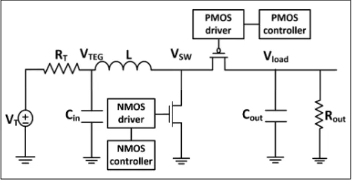
Fig. 1. Boost converter block diagram.
그림 1. 부스트 컨버터 회로도
Ⅰ. 서론
Zero Current Sensor (ZCS)는 Discontinuous Conduction Mode (DCM)를 지원하는 boost converter가 정상적으로 동작하기 위해 중요하다.
Boost converter에서 ZCS는 인덕터에 저장되어 있던 전류를 load쪽으로 보낼 때 전류가 다 전달 되어 전류가 0인 순간을 알려주는 block이다. [1]
[4] ZCS가 전류가 0인 시점을 정확하게 찾을수록 Zero Current Switching 동작을 제때 할 수 있으 며 효율 또한 높아진다. 일반적으로 사용되는 다 양한 ZCS 방법들은 power소모, 정확도, area등 에서 단점을 가지고 있다. 본 논문에서는 기존에 사용되는 ZCS방법들 보다 power소모를 줄이고 정확도를 높인 새로운 구조를 제안하고자 한다.
Ⅱ. 본론
1. 기존의 ZCS 방법들
일반적인 ZCS 방법으로는 clk 기반의 comparator를 이용하거나 [1], analog comparator [2], delay line [3] 등을 이용한 방법들이 있다. 그 러나 이 방법들은 각각의 단점을 가지고 있다.
Clk 기반의 comparator는 전류가 0인 시점을 빠 르고 정확하게 잘 찾아내지만 power 소모가 큰 단점이 있다. Analog comparator는 power 소모는 적지만 comparator의 두 입력이 같은 순간으로부 터 결과가 나오기 까지 오랜 시간이 걸리고 결과 를 빨리 나오게 하려면 많은 전류를 사용해야하 므로 power 소모가 증가한다. delay line을 사용 하는 ZCS방법은 수많은 gate들이 들어가기 때문 에 area측면에서 큰 단점을 가지고 있다.
Fig. 2. Offset controlled V_load waveform 그림 2 Offset controlled V_load 파형도
2. 제안하는 ZCS 방법 가. 새로운 ZCS 동작 원리
이 논문에서 제안할 새로운 ZCS 구조는 analog comparator를 이용한 ZCS 구조와 delay line을 이용한 ZCS 구조의 장점들을 이용해 만든 구조이 다. Delay line은 코드로 delay의 정도를 조절하여 전류가 0인 순간을 맞추어 간다. 그러나 새로 제 안할 구조는 analog comparator 구조에 delay line처럼 코드를 이용하여 offset의 정도를 조절하 는 것이다. 그림 2.처럼 offset의 정도를 조절하여 V
SW와 V
load가 만나는 지점을 조절한다. V
SW와 V
load가 만나는 지점이 V
load_offset으로 조절되면 comparator의 출력이 나오는 시점이 조절되므로 offset을 조절하여 PMOS on time을 조절 할 수 있다.
제안하는 구조는 analog comparator를 이용한 ZCS 구조 보다 더 적은 power를 사용하고 delay line을 이용한 ZCS 구조보다 더 적은 면적을 사 용하며 전류가 0인 지점을 정확하게 찾아갈 수 있다. 그림 3.은 새롭게 제안하는 offset controlled 방식의 ZCS의 회로도 이다. 그림 3.을 보면 analog comparator 구조를 기반으로 6bit 코드를 사용하여 offset이 조절가능하게 만든 것을 알 수 있다. 입력신호가 들어오는 MOS들은 코드와 맞 게 Size를 binary로 설정하였다. 입력되는 코드가 낮을수록 연결되는 MOS가 적어지고 offset의 정 도가 커지게 되므로 출력이 더 빠르게 나와 Zero Current Switching 하는 순간을 앞당기게 된다.
입력되는 코드가 높을수록 연결되는 MOS가 많아
지고 offset의 정도가 작아지게 되므로 출력이 더
늦게 나와 Zero Current Switching 하는 순간이
뒤로 더 밀어지게 된다.
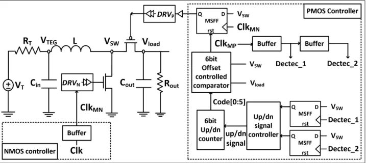
Fig. 3. Block diagram of offset controlled Comparator 그림 3 offset controlled Comparator 구조 회로도
나. 새로운 ZCS 동작 구현
새로운 ZCS 구조로 인덕터 전류가 0인 지점을 정확히 찾기 위해서는 현재 PMOS 스위치가 인 덕터 전류가 0인 지점보다 연결이 빨리 끊겼는지 늦게 끊겼는지 여부를 아는 것이 중요하다. 그 여 부는 V
SW의 상태를 보고 파악 할 수 있다.
PMOS 스위치가 늦게 닫힌 경우에는 V
SW노드가 아래로 떨어지게 된다. PMOS 스위치가 빨리 닫 힌 경우에는 V
SW노드가 위로 올라가게 된다. 따 라서 V
SW노드의 상태를 감지하여 코드를 어떻게 조절 할지 여부를 결정할 수 있다. 그림 4.처럼 Detec_1, Detec_2 신호로 V
SW노드의 순간 값을 가져오고 두 값을 게이트로 이루어진 회로를 통 해 up/down 카운터를 up으로 동작시킬지 down 으로 동작시킬지 결정한다. 카운터가 up 이나 down으로 동작한 이후 6bit의 결과를 offset controlled ZCS에서 사용하는 comparator에 넘겨 주면 offset의 정도를 정하여 PMOS의 on time인 Clk
MP를 결정한다. Detec_1이 시작, Detec_2가 끝 인 윈도우를 만들고 V
SW에 윈도우를 적용한다.
그림 4.(a)처럼 윈도우 보다 앞에서 V
SW가 1에서 0으로 바뀌면 offset을 줄이고 그림 4.(b)처럼 윈 도우 보다 뒤에서 V
SW가 1에서 0으로 바뀌면 offset을 늘린다. 그림 4.(c)처럼 윈도우 안에서 V
SW가 1에서 0으로 바뀌면 offset을 유지한다.
Fig. 4. Boost converter circuit waveforms when detect operation.
그림 4. 감지 동작 할 때의 부스트 컨버터 파형도
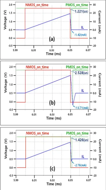
Fig 5. MOS on time and Inductor current in each Zero Current Switching methode.
그림 5. 각각 다른 Zero Current Switching의 MOS 동작
시간과 인덕터 전류
Fig. 6. Block diagram of Boost converter using offset controlled ZCS
그림 6. offset controlled ZCS를 사용하는 부스트 컨버터 회로도
다. 다른 ZCS 구조와 비교
그림 5는 동일한 상황에서 다른 ZCS 구조를 비 교하기 위한 결과이다. 표 1.은 다른 ZCS 구조를 bias전압, power, PMOS on time, 인덕터 전류의 negative peak 전류 등을 정리한 표이다. 그림 6 은 제안하는 구조의 전반적인 회로도이다.
그림 5.(a)는 새로 제시한 ZCS구조의 PMOS, NMOS 스위칭 시간과 인덕터 전류 그래프이다.
그림 5.(b)는 analog comparator 이용하여 새로 제시한 ZCS구조와 같은 값의 bias 전압을 걸어서 같은 전류량을 사용했을 때 결과이다. 그림 5.(c) 는 analog comparator를 이용하여 새로 제시한 ZCS구조와 비슷한 PMOS on time 결과를 만들 어내기 위해 bias전압을 조절해 전류량을 증가시 킨 결과이다.
그림 5.(a)와 그림 5.(c)처럼 새로운 ZCS 구조 와 비슷한 결과를 analog comparator로 얻기 위 해서는 표 1.처럼 더 많은 전류량이 필요하다. 하 지만 사용하는 power의 양은 10배 정도 차이가 난다. 새로운 ZCS구조와 같은 양의 전류량으로 analog comparator를 동작시키면 사용하는 power 의 양은 비슷하지만 PMOS 스위칭 동작을 그림 5(a)의 스위칭 시간보다 그림 5(b)의 스위칭 시간 이 대략 2배 정도 차이가 나는 것을 알 수 있다.
Delay line은 성능적인 면에서는 새로 제시한 ZCS 구조와 비슷하지만 delay를 조절하기 위해서 수많은 gate들이 들어간다. Inverter나 nand gate 를 이용하여 delay line을 만들면 보통 수십 pico 단위의 delay 밖에 걸리지 않기 때문에 그림 5.(a) 와 비슷한 1.2u 정도의 시간을 delay line으로 설 계하기 위해서는 많은 면적이 필요하다. [3] 또한 delay line은 delay range를 정하여 설계를 진행하 면 이후에는 그 이상의 범위를 조절 할 수 없다.
따라서 Zero Current Switching에 필요한 p_on_time의 pulse width가 delay range를 벗어나 면 항상 손실이 발생한다. 하지만 새로 제시한 ZCS 구조는 analog comparator를 기반으로 offset을 조절하기 때문에 Zero Current Switching에 필요한 p_on_time의 pulse width가 길어도 Zero Current Switching이 가능하다.
Table 1. Power comparison of new ZCS and analog comparator.
표 1. 새로운 ZCS 구조와 아날로그 비교기 ZCS 구조의
파워 비교
에서 장점을, delay line보다 area에서 장점을 가 지고 delay line과 달리 delay range에 의한 제약 을 받지 않는다. 이처럼 새롭게 제시한 ZCS 구조 를 이용하여 Zero Currnet Switcing 동작을 했을 때 정확하고 더욱 높은 효율의 boost converter 동작을 구현할 수 있다.
References