Vol.19, No.3, (2017), pp.18~22 http://dx.doi.org/10.9714/psac.2017.19.3.018
```
1. INTRODUCTION
In addition to YBa2Cu3O7-δ (YBCO), REBa2Cu3O7-δ
(REBCO: RE = Er, Nd, Gd, and Sm) superconductors are being studied extensively for power applications because of larger critical current density and stronger pinning property at liquid nitrogen temperature and under magnetic field than those of YBCO [1]. In order to effectively increase the critical current density, magnetic flux pinning centers are needed to control the flux flow. The addition of artificial pinning centers may enhance the pinning force against the Lorentz force and suppress the magnetic flux flow. It has been reported that the critical current density can be improved when BaMO3 (M = Zr, Sn, and Hf, BMO) acting as an artificial pinning center is added to YBCO and REBCO [2-6]. BMO is found to form 1-dimensional nanostructures inside the film and to act as effective pinning centers resulting an enhanced flux pinning.
Recently the addition of BaSnO3(BSO) to YBCO and NdBa2Cu3O7-δ (NdBCO) has been reported [7-9].
BMO addition to GdBa2Cu3O7-δ (GdBCO) has also been studied widely. In previous experiments, we studied the thickness dependence of critical current density of 2 wt. % of BSO-added GdBCO films [10-13]. It was found that by the addition of BSO, 1-dimensional nanostructures were formed along the thickness of the film and the critical current density was mostly improved at thickness between 600 nm and 800 nm [13]. Motivated by these results, we fabricated 4 wt. % BSO-added GdBCO target to study the correlation of the BSO growth and the pinning property of
GdBCO. It was reported that 4 wt. % BSO addition largely improved the critical current density of YBCO [7, 13].
In this study, we investigated the effect of deposition conditions, temperature and the repetition rate of laser pulse, on the growth of BSO which affects the pinning properties of GdBCO thin films.
2. EXPERIMENTAL
The GdBCO thin films doped with 4 wt.% BSO were deposited on a SrTiO3 (STO) (100) substrate by pulsed laser deposition (PLD) process using excimer laser (KrF, λ
= 248 nm). Thin film deposition was performed using a laser energy of 180 mJ, oxygen partial pressure of 400 mTorr and the final thicknesses of films are ~ 700 nm. For varying temperature, deposition temperature of substrate was varied from 700 °C to 810 °C and the repetition rate was kept to be 3 Hz. For varying repetition rate, the deposition temperature was fixed at 750 °C and the repetition rate was varied from 3 Hz to 15 Hz, respectively.
After the deposition, post-heat treatment was performed in an oxygen atmosphere at 500 °C and 500 Torr for 1 hour.
The surface and the cross-sectional morphologies and crystal structures of the fabricated films were examined by scanning electron microscope (SEM) and X-ray diffraction (XRD) 2-theta scan analysis. In order to check the morphology inside the films, ion-milling experiments were carried out. Ion-milling is advantageous in that it is easy to measure the two-dimensional nanostructure distribution with respect to the thickness variation of the measurement sample. The argon ion beam and the sample were placed
The flux pinning properties of BaSnO
3-added GdBa
2Cu
3O
7-δfilms with varying growth conditions
J. K. Lee a, J. Y. Oh a, J. M. Lee b, W. N. Kang b, and B. Kang a,*
a Department of Physics, Chungbuk National University, Cheongju, Korea
b Department of Physics, Sungkyunkwan University, Suwon, Korea
(Received 2 August 2017; revised or reviewed 4 September 2017; accepted 5 September 2017)
Abstract
Addition of BaSnO3 (BSO) to GdBa2Cu3O7-δ (GdBCO) is reported to enhance the flux pinning property of GdBCO thick films.
To investigate the effect of growth condition on the pinning properties, 700 nm-thick BSO-added GdBCO films deposited with varying temperatures and growth rates were prepared by using a pulsed laser deposition method. As the deposition temperature increases, the critical current density and the pinning force density show an improved field dependence up to 750 ℃ due to th e increase in the formation of the a-axis growth and the BSO nanostructures. The films deposited at higher temperatures show degraded surfaces and as a result, degraded pinning behaviors. For the change in growth rate, the critical current density and the pinning force increase as the repetition rate increase at low magnetic fields, but this behavior is reversed in high magnetic fields.
These results indicate that the film growth conditions significantly affect the formation of BSO nanostructures and the pinning properties of BSO-added GdBCO films.
Keywords: GdBCO, BSO, pinning property, repetition rate
* Corresponding author: [email protected]
vertically and about 200 nm of the films was etched with an energy of 3 keV and then, the films were further etched with 300 eV energy to remove an uneven portion of the surface. The critical current density was deduced from the magnetization measurement conducted at 65 K and 77 K by using a magnetic property measurement system (MPMS) in magnetic fields applied parallel to the c-axis of the films.
3. RESULTS AND DISCUSSION 3.1. Varying Deposition Temperature
To investigate the flux pinning property of BSO-added GdBCO films deposited at different temperatures, the field dependence of the critical current density was examined.
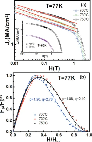
Fig. 1. The field dependence of (a) the critical current density and (b) the normalized pinning force density of the BSO-added GdBCO thin films deposited at varying temperature. The solid and dotted lines are fitting lines.
TABLE. 1.
THE P, Q VALUES AND THE PINNING FORCE DATA OBTAINED FROM THE FIT TO THE DEW-HUGHES MODEL WITH TEMPERATURE CHANGE ARE SHOWN.
Temperature (°C) 700 730 750
α (77 K) 0.21±0.02 0.22±0.02 0.19±0.01
p 1.20 1.10 1.08
q 2.78 1.95 2.10
Hmax (T) 1.10 1.15 1.25
(H/Hirr)max 0.28 0.32 0.34
Fig. 1 (a) shows the double logarithmic plot of Jc versus H of the BSO-added GdBCO films deposited at different temperature. The critical current density was calculated using the simplified Bean’s model by 𝐽𝑐 = 20∆𝑀 [𝑏(1 − 𝑏 3𝑎⁄ ⁄ )] [10, 14], where ΔM is the difference of magnetization when the magnetic field is increased or decreased, and a and b are the width and the length of the rectangular sample, respectively. As the deposition temperature increases up to 750 °C, the critical current density tends to increase, and the film deposited at 750 °C has the highest critical current density of 5.80 MA/cm2. In the literature, the double-logarithmic plot of Jc
vs. H is usually separated into two regions [15-17]. In the low-field region, where vortices are individually pinned, the field-independent Jc’s are obtained. In the intermediate-field region, the vortices collectively interact each other as the vortex density becomes greater than the defect density. In this region, the flux pinning mechanism is represented by the exponent α in the power law of 𝐽𝑐~𝐻−𝛼 . For the case of PLD-REBCO, the values of α ~ 0.5 have been reported which implies a relatively diluted distribution of extended defects. In our previous studies on the critical current density of GdBCO films with varying thickness, we have observed α ~ 0.5 for the 200 nm- and 1000 nm-thick films, and a smaller value of α ~ 0.35 for the 600 nm-thick film, respectively [13]. For the BSO-added GdBCO, the values of α were found to be much smaller than that of GdBCO, α = 0.21 ± 0.02 for the film deposited at 700 °C and systematically decreased to 0.19 ± 0.01 for 750 °C. Reduced values of α with increasing deposition temperature indicate that more effective pinning has occurred in the film of 750 °C, which agrees with the larger values of Jc. Further increase of deposition temperature to 780 °C lead to deterioration of superconducting properties, so the critical current density could be measured only at 65 K. The inset of Fig. 1(a) shows comparison of field dependences of Jc vs. H for the films deposited at 750 °C and 780 °C. As expected, Jc of the film for 780 °C exhibited low values as well as poor field dependence.
The pinning force density Fp (𝐹𝑝= 𝐽𝑐× 𝜇0𝐻), deduced from the Jc vs. H data may deliver more information on the pinning mechanism. Fig. 1 (b) represents the normalized pinning force density as a function of reduced field H/Hirr
and the irreversibility field Hirr was determined by using a criteria of 𝐽𝑐= 1000 𝐴 𝑐𝑚⁄ 2. In order to investigate pinning mechanism, the data were fit to the formula, 𝐹𝑝/𝐹𝑝𝑀𝑎𝑥 ~ ℎ𝑝(1 − ℎ)𝑞 of Dew-Hughes model [18], where p and q are characteristic exponents reflecting pinning types and the solid and the dotted lines are the fit.
The exponents and other parameters from the fit are listed in Table. 1. The normalized pinning force density of the films deposited at 730 °C and 750 °C show a very similar shape while that of the film of 700 °C is different. As a result, the exponents for 730 °C and 750 °C are very close, but different from those for 700 °C indicating different pinning mechanism.
The value of Hmax, the magnetic field for 𝐹𝑝𝑚𝑎𝑥, increases as the deposition temperature increase. For example, it is 1.10 T at 700 °C and increases to 1.25 T at 750 °C, implying stronger pinning at higher magnetic field.
Fig. 2. The surface SEM images after ion-milling for (a) 730 °C, (c) 780 °C and the cross-section SEM image of (b) 730 °C and, (d) 780 °C.
An examination of nanostructure inside the films was conducted by ion-milling process and SEM studies. Figure 2 (a)-(d) are a comparison of surface and cross-sectional SEM images of the ion-milled films deposited at 730 °C and 780 °C. For the film of 730 °C, grain boundaries (marked by yellow arrow) starting from the middle of the film as well as nanorods, which may serve as pinning centers [11], were observed. On the other hand, for the film deposited at 780 °C, the surface began to partially melt and cracks (marked by blue arrow) starting from the intersection of substrate/film were observed. From this result, it is concluded that the optimal temperature for the BSO growth is near 750 °C in our system and the well grown BSO nanostructure could enhance the pinning property of GdBCO films.
3.2. Varying Repetition Rate
For the 2nd set of experiment, the deposition temperature is kept at 750 °C where the growth of BSO nanostructure is most effective, and the repetition rate of laser was changed from 3 Hz, 6 Hz, 10 Hz, and 15 Hz while the thicknesses of
Fig. 3. The ion-milled SEM image of the films with the varying repetition rate of (a) 3Hz, (b) 6Hz, (c) 10Hz, and (d) 15Hz.
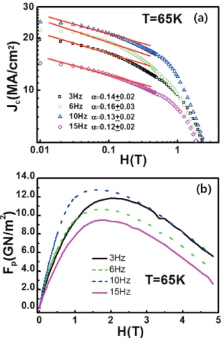
Fig. 4. The field dependence of (a) the critical current density and (b) the pinning force measured at T = 65K with varying repetition rates.
the films were maintained to be ~700 nm. The SEM images of the films are shown in Fig. 3 (a)-(d). It can be seen that as the repetition rate increases, the amount of BSO nanostructures (marked by rectangular box) and a-axis growths observed on the surface of the films decrease and at the surface of 15 Hz, BSO nanostructures are not observed. This result suggests that BSO growth can be controlled by the repetition rate [19]. It is noteworthy that unlike films with 6 Hz-15 Hz, the SEM image for the 3 Hz film exhibits short length grain boundaries (marked by arrow in the circle) as well as BSO nanostructures.
The influence of the surface morphology on the Jc was investigated. Figure 4 (a) shows the field dependence of the critical current density measured at T = 65 K for the films with different repetition rates. As the repetition rate increases, the Jc systematically increases up to 10 Hz, and then decreases for the film with 15 Hz. As a result, the film with 10 Hz has the highest value of Jc and the best field performance in the whole field region and the film with 6 Hz is the next. The Jc values of the film with the lowest repetition rate of 3 Hz are smaller than those of 6 Hz at low field region, but they surpass those of 6 Hz at high field region. This behavior can be clearly seen in the field dependence of Fp as shown in Fig. 4 (b). The Fp of 3 Hz surpass that of 6 Hz near at 1 T and becomes similar to that of 10 Hz at 2.8 T. Another interesting feature of Fp is the field of Fpmax (Hmax). The values of Hmax are 2.0 T, 1.7 T,
Fig. 5. Comparison of the field dependence of Jc of the films with repetition rates of 3 Hz and 10 Hz at 77 K. Inset:
Comparison of the field dependence of Fp of the films with 3 Hz and 10 Hz at 65 K.
1.7 T, and 1.8 T for 3 Hz, 6 Hz, 10 Hz, and 15 Hz, respectively. In general, shift of Hmax to higher/lower field indicates more/less effective pinning, so the pinning mechanism of the film with 3 Hz seem to be different from other films.
To find the reason for the difference, the Jc and Fp data of 3 Hz and 10 Hz are compared in Fig. 5. As shown in Fig. 5, the Jc’s of 10 Hz at 77 K are higher than those of 3 Hz up to H* = 1.3 T and then become smaller than those of 3 Hz.
The H* at which a crossover occurs can be compared with the matching field 𝐻Φ= 𝑛Φ0 , where Φ0 is the fluxon and n is the density of pinning centers. The density of pinning centers is estimated from the volume fraction of the grain size D of BSO obtained by using the Scherrer equation [20]
and this gives HΦ = 0.5 T and 0.7 T for the films with 3 Hz and 10 Hz, respectively. The value of H* is larger larger than that of HΦ for 10 Hz and the reason for this may be the fact that more than one vortex are trapped in pinning centers with sizes much larger than those of the vortices.
The typical diameter of a vortex core is given by 2ξ, with ξ being the coherence length of the GdBCO superconductor.
The temperature dependence of ξ is expressed as ξ = ξ0 (1 − T/Tc)−0.5 [21], where ξ(0)~2 nm [22]. The Tc's of the BSO-added GdBCO films with 3 Hz and 10 Hz films are found to be around 90 K from the magnetization measurements (not shown here); hence, the vortex size 2ξ at 77 K is calculated to be 9.4 nm. The estimated grain sizes of BSO are to be 25 nm and 21 nm for the 3 Hz and the 10 Hz, respectively. As a result, the number of vortices pinned by each BSO could be multiple, which leads to H* ~ 2HΦ of the 10 Hz film.
The inset of Fig. 5 illustrates the Fp data of the 3 Hz and the 10 Hz films measured at 65 K. Similar to the data measured at 77 K, the Fp’s of 10 Hz are higher than those of 3 Hz up to H* = 2.8 T, then they become the same with those of 3 Hz. The value of H* = 2.8 T is much larger and H* ~ 4HΦ of the 10 Hz film. At this temperature,the size of vortex core is estimated to be ~ 6.8 nm [23] which is much smaller than the BSO grain size. These analyses imply that for the film with 10 Hz, BSO nanostructures act as effective pinning centers while for the film with 3 Hz,
other pinning centers, such as grain boundaries, also exist and play an important role at high magnetic fields.
4. SUMMARY
We investigated the effect of BSO growth condition on the critical current density of 4 wt.% BSO-added GdBCO with varying deposition temperatures and repetition rates.
By varying temperature, the critical current density tended to increase from 700 °C to 750 °C because the length of BSO nanostructure increases with increasing temperature.
However, at higher temperatures, the critical current density was reduced because of the melted surface and the cracks formed due to high temperature. As a result, a temperature of 750 °C is found to be the optimal condition for the critical current density of BSO-added GdBCO.
In the case of repetition rate change, 10 Hz is observed to be optimal to have high critical current density in whole magnetic field region. However, pinning of the 3 Hz film is found to be effective in high field region which may be attributed to the coexisting of BSO nanostructures and the grain boundaries. It is found that the growth of BSO nanostructures could be controlled by the repetition rate.
ACKNOWLEDGMENT
This work was supported by the Basic Science Research Program through the National Research Foundation of Korea (NRF) funded by the Ministry of Education Science (NRF-2015R1D1A3A01019291).
REFERENCES
[1] David Larbalestier, Alex Gurevich, D. Matthew Feldmann and Anatoly Polyanskii, “High-Tc superconducting materials for electric power applications,” Nature., vol. 414, pp. 368-377, 2001.
[2] J. Gutiérrez, A. Llordés, J. Gázquez, M. Gibert, N. Romà, S. Ricart, A. Pomar, F. Sandiumenge, N. Mestres, T. Puig and X. Obradors,
“Strong isotropic flux pinning in solution-derived YBa2Cu3O7-x
nanocomposite superconductor films,” Nature Materials, vol. 6, pp.
367-373, 2007.
[3] M. Erbe, J. Hänisch, R. Hühne, T. Freudenberg, A. Kirchner, L.
Molina-Luna, C. Damm, G. Van Tendeloo, S. Kaskel, L. Schultz and B. Holzapfel, “BaHfO3 artificial pinning centres in TFAMOD-derived YBCO and GdBCO thin films,” Supercond. Sci.
Technol., vol. 28, pp. 114002, 2015.
[4] T. Matsushita, H. Nagamizu, K. Tanabe, M. Kiuchi, E. S. Otabe, H.
Tobita, M. Yoshizumi, T. Izumi, Y. Shiohara and D. Yokoe,
“Improvement of flux pinning performance at high magnetic fields in GdBa2Cu3Oy coated conductors with BHO nano-rods through enhancement of Bc2,” Supercond. Sci. Technol., vol. 25, pp. 062002, 2012.
[5] Satoshi Awaji, Masafumi Namba, Kazuo Watnabe, Shun Ito, Eiji Aoyagi, Hideki Kai, Masashi Mukaida and Ryusuke Kita, “Flux pinning properties in BaMO3 (M=Zr,Sn) nanorod-introduced ErBa2Cu3Ox films,” Journal of Applied Physics, vol. 106, pp.
103915, 2009.
[6] Tomoya Horide, Kenta Taguchi, Kaname Matsumoto, Naoki Matsukida, Manabu Ishimaru, Paolo Mele and Ryusuke Kita,
“Influence of matching field on critical current density and irreversibility temperature in YBa2Cu3O7 films with BaMO3
(M = Zr, Sn, Hf) nanorods ,” Appl. Phys. Lett., vol. 108, pp.
082601, 2016.
[7] P. Mele, K. Matsumoto, A. Ichinose, M. Mukaida, Y. Yoshida, S.
Horii and R. Kita, “Systematic study of the BaSnO3 insertion effect on the properties of YBa2Cu3O7−x films prepared by pulsed laser ablation,” Supercond. Sci. Technol., vol. 21, pp. 032002, 2008.
[8] Kaname Matsumoto, Isamu Tanaka, Tomoya Horide, Paolo Mele, Yutaka Yoshida and Satoshi Awaji, “Irreversibility fields and critical current densities in strongly pinned YBa2Cu3O7-x films with BaSnO3 nanorods: The influence of segmented BaSnO3 nanorods,”
Journal of Applied Physics, vol. 116, pp. 163903, 2014.
[9] Y. Tanaka, M. Mukaida, R. Teranishi, K. Yamada, A. Ichinose, K.
Matsumoto, S. Horii, Y. Yoshida, R. Kita, T. Fujiyoshi and N. Mori
“Fabrication and characterization of BaSnO3-doped NdBa2Cu3O7-d
thin film,” Physica C, vol. 468, pp. 1864-1868, 2008.
[10] D. H. Tran, W. B. K. Putri, C. H. Wie, B. Kang, N. H. Lee, W. N.
Kang, J. Y. Lee and W. K. Seong, “Thickness dependence of critical current density in GdBa2Cu3O7−δ thin films with BaSnO3 addition,”
Journal of Applied Physics, vol. 111, pp. 07D714, 2012.
[11] D. H. Tran, W. B. K. Putri, B. Kang, N. H. Lee, W. N. Kang and W.
K. Seong, “Reducing thickness dependence of critical current density in GdBa2Cu3O7-δ thin films by addition of nanostructured defects,” Journal of Applied Physics, vol. 113, pp. 17E134, 2013.
[12] D. H. Tran, W. B. K. Putri, B. Kang, N. H. Lee and W. N. Kang, “A close correlation between nanostructure formations and the thickness dependence of the critical current density in pure and BaSnO3-added GdBa2Cu3O7-δ films,” Journal of Applied Physics, vol. 115, pp. 163901, 2014.
[13] Duc H. Tran, Witha B. K. Putri, Byeongwon Kang, Nam Hoon Lee and Won Nam Kang, “The Critical Current Density of GdBa2Cu3O7−δ Superconducting Films: Thickness, Temperature, and Field Dependences,” IEEE Trans. on Mag., vol. 50, 2014.
[14] X. L. Wang, A. H. Li, S. Yu, S. Ooi, K. Hirata, C. T. Lin, E. W.
Collings, M. D. Sumption, M. Bhatia, S. Y. Ding and S. X. Dou,
“Thermally assisted flux flow and individual vortex pinning in Bi2Sr2Ca2Cu3O10 single crystals grown by the traveling solvent floating zone technique,” J. Appl. Phys., vol. 97, pp. 10B114, 2005.
[15] S. R. Foltyn, L. Civale, J. L. MacManus-Driscoll, Q. X. Jia, B.
Maiorov, H. Wang and M. Maley, “Materials science challenges for high-temperature superconducting wire,” Nature Materials, vol. 6, pp. 631- 642, 2007.
[16] J. Gutierrez, A. Llordes, J. Gazquez, M. Gibert, N. Roma, S. Ricart, A. Pomar, F. Sandiumenge, N. Mestres, T. Puig and X. Obradors,
“Strong isotropic flux pinning in solution-derived YBa2Cu3O7−x
nanocomposite superconductor films,” Nature Materials, vol. 6, pp.
367-373, 2007.
[17] B. Dam, J. M. Huijbregtse, F. C. Klaassen, R. C. F. van der Geest, G.
Doornbos and J. H. Rector, et al., “Origin of high critical currents in YBa2Cu3O7−δ superconducting thin films,” Nature, vol. 399, pp.
439-442, 1999.
[18] Dew-Hughes, “Flux pinning mechanism in type II superconductors,”
Phil. Mag., vol. 30, pp. 293, 1974.
[19] B. Maiorov, S. A. Baily, H. Zhou, O. Ugurlu ,J. A. Kennison, P. C.
Dowden, T. G. Holesinger, S. R. Foltyn and L.Civale, “Synergetic combination of different types of defect to optimize pinning landscape using BaZrO3-doped YBa2Cu3O7,” Nature Materials, vol.
8, pp. 398-404, 2009.
[20] J. I. Langford and A. J. C. Wilson, “Scherrer after sixty years: A survey and some new results in the determination of crystallite size,”
J. Appl. Cryst., vol. 11, pp. 102-113, 1978.
[21] G. Blatter, M. V. Feigel'man, V. B. Geshkenbein, A. I. Larkin and V.
M. Vinoku, “Vortices in high-temperature superconductors,” Rev.
Mod. Phys., vol. 66, pp. 1125, 1994.
[22] Alexey V. Pan, A. Serhiy Pysarenko and Shi X. Dou, “Drastic improvement of surface structure and current-carrying ability in YBa2Cu3O7 films by introducing multilayered structure,” Appl.
Phys. Lett., vol. 88, pp. 232506, 2006.
[23] D. R. Nelson and V. M. Vinokur, “Boson localization and correlated pinning of superconducting vortex arrays,” Phys. Rev. B, vol. 48, pp. 13060, 1993.