Vol.19, No.3, (2017), pp.13~17 http://dx.doi.org/10.9714/psac.2017.19.3.013
```
1. INTRODUCTION
For practical application of ReBa2Cu3O7-x (REBCO, RE
= Y, Sm, Gd, etc) superconducting films, large critical current density (Jc) and large pinning force maximum (Fp.max) are required in high magnetic fields. In general, REBCO thin films have high Jc values due to intrinsic pinning centers such as crystalline defects generated inside the films during the film fabrication [1-4]; however, a drastic reduction in Jc at high magnetic fields still remains a problem.
Among various candidates for overcoming Jc decrease at high fields, inserting second phase in the film as a pinning center is known to be very effective [5-7]. Enhancement of Jc at high magnetic fields can be accomplished by introducing artificial pinning centers (APCs) in HTS films with controlled dimensionality [6]. Especially, the insertion of APCs such as BaMO3 (BMO, M = Zr [10], Hf [10-11], and Sn [12]) confirmed that self-assembled BaMO3 nanorods with diameter of ~10 nm were formed parallel to the c-axis of the films [10-12]. This c-axis correlated pinning center of dopants resulted in a drastic improvements of both Jc and the pinning force at high magnetic fields [7-9, 13]. Enhanced flux pinning by BMO nanorods is quite fascinating from a power application point of view, but the pinning mechanism is not quite clearly understood yet.
In our previous work, we have reported that the thickness dependence of Jc in the GdBCO films was weakened by adding 2 wt. % BSO as second phase [12].
Motivated from this result, we investigated the thickness dependence of pinning mechanism in 4 wt. % (3.5 vol. %)
BSO-added GdBCO thin films. In order to identify the source of dominant pinning and to compare intrinsic and artificial pinning center, we concentrated on comparison of pinning performance analyzed by the Dew-Hughes’
theoretical prediction.
2. EXPERIMENT
GdBCO films containing 3.5 vol. % BSO with thickness from 200 nm to 1000 nm were deposited on SrTiO3 (STO) single crystal substrates by using a PLD (KrF excimer laser: λ = 248 nm) method. BSO was incorporated into the GdBCO films in a manner of premixing the target before sintering [14]. The substrate temperature, O2 partial pressure, laser energy and frequency were set to 700 ℃, 400 mTorr, 150 mJ, and 10 Hz, respectively. After the deposition, all of the films were annealed at 500 ℃ in 500 Torr oxygen for an hour and cooled to room temperature.
Crystalline structure of the film was investigated by x-ray diffraction (XRD, Cu Kα: λ = 1.54 Å) and the critical temperature (Tc) was measured by a four-point probe method. Magnetization of the GdBCO films were measured at 77 K and 65 K by a Magnetic Property Measurement System (MPMS, Quantum Design XL-5) in magnetic fields up to 5 T applied to the c-axis of the film.
The Jc values of films were calculated by the equation of Jc= 20 △ 𝑀/[𝑏 �1 −3𝑎𝑏�] from the Bean’s critical state model [15], where △ 𝑀 is the magnetization hysteresis loop width per unit volume, and a and b are the dimensions of the rectangular samples (a < b).
Effect of double pinning mechanism in BSO-added GdBa
2Cu
3O
7-xthin films
J. Y. Oha, H. K. Jeona, J. M. Leeb, W. N. Kangb, and B. Kang a,*
a Department of Physics, Chungbuk National University, Cheongju, Korea
b Department of Physics, Sungkyunkwan University, Suwon, Korea
(Received 7 July 2017; revised or reviewed 13 September 2017; accepted 14 September 2017)
Abstract
We investigated the effect of self-assembled BSO nano-defects as pinning centers in BSO-added GdBCO films when the thicknesses of films were varied. 3.5 vol. % BSO-added GdBCO films with varying thicknesses from 200 nm to 1000 nm were deposited on SrTiO3 (STO) substrate by using pulsed laser deposition (PLD) process. For the films with thicknesses of 400 nm and 600 nm, ‘anomaly shoulders’ in Jc - H characteristic curves were observed near the matching field. The anomaly shoulders appeared in the field dependence of Jc may be attributed to the existence of double pinning mechanisms in thin films. The fit to the pinning force density as a function of reduced field h (H/Hirr) using the Dew-Hughes’ scaling law shows that both the 400 nm- and the 600 nm-thick films have double pinning mechanisms while the other films have a single pinning mechanism. These results indicate that the self-assembled property of BSO result in different role as pinning centers with different thickness.
Keywords: GdBCO, BSO, nano defects, artificial pinning centers, pinning mechanism
* Corresponding author: [email protected]
3. RESULTS AND DISCUSSION
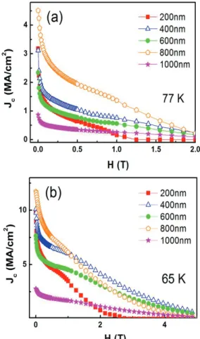
The critical current densities (Jc) as a function of applied magnetic field of BSO-added GdBCO films with different thickness are compared at (a) 77 K and (b) 65 K in Fig. 1. It is indicated that at 77 K, Jc of ~ 4.5 MA/cm2 for 800 nm- thick film is the highest value in the whole range of the applied field. On the contrary to Jc at 77 K, Jc at 65 K shows different tendency. Both the 400 nm-thick and the 600 nm-thick films have higher Jc values than the 800 nm- thick film in high magnetic field region. The Jc-H curve of the 400 nm- and the 600 nm-thick films at 65K exhibited anomaly shoulders near 1.0 T. Similar behavior has been observed in GdBCO + Gold film by T. Horide et al. [16].
Different field dependences of Jc at different temperatures indicate that pinning mechanism may change as the film thickness increases at different temperatures. In order to figure out pinning mechanism at different thickness of the films, systematic analyses on the crystalline structure and the pinning force density are essential.
Crystalline structure of the BSO-added GdBCO films was firstly examined as represented in the inset of Fig. 2.
GdBCO (0 0 l) peaks with large intensity and no additional a-axis peak indicate that all the GdBCO films are completely c-axis oriented [17]. Fig. 2 shows the normalized FWHM values of BSO calculated by (005) peak and Jc at 77 K plotted as a function of film thickness.
As shown in Fig. 2, Jcs at 77K are inversely related to
Fig. 1. Critical current densities (Jc) of the BSO-added GdBCO film at (a) 77 K and (b) 65 K in magnetic fields parallel to the c-axis.
Fig. 2. Normalized FWHM and Critical current density (Jc) at 77K plotted as a function of film thickness, and inset shows X-ray diffraction (XRD) patterns for all films.
the normalized FWHM values of BSO (200) peak which was normalized by maximum intensity of GdBCO(005) at each thickness. This result agrees with the report that sharpness of BSO FWHM values which signifies good crystallinity of BSO results in large value of Jc of the film [18]. We have also reported that enhanced pinning can be achieved when relative crystallinity of BSO nano defects to GdBCO is superior [17]. This result implies that Jc at 77K is dominantly determined by crystalline BSO.
To learn more about the pinning properties in the GdBCO films, we calculated the parametric variable of the films such as BSO grain size and the coherence length. The BSO grain size D and the coherence length ξ for each film can be calculated by using the Scherrer equation and the Ginzburg-landau equation [19, 20]:
D = 0.9λ/βcosθ (1) ξ = ξ0 (1 − T/Tc)−0.5 (2) where λ is the x-ray wavelength, β is the FWHM values in radians, θ is the half angle for maximum intensity position, and ξ0 is coherence length at 0 K: for GdBCO, it is well known that ξ0 = 1.8 nm [21]. Calculated parameters are listed in Table. 1.
The average grain size of BSO is ~20 nm and the coherence lengths of films are ~5.0 nm at 77 K and ~3.5 nm at 65 K, except those of 1000 nm- thick film (~9.2 nm at 77 K and ~4.0 nm at 65 K). In general, if flux pinning center is much larger than the size of flux, which is considered to be two times of the coherence length of the film, one or more flux can be trapped in the flux pinning center [2, 22]. Comparing the average grain size and the coherence length, BSO nano-defects are suitable for trapping quantized flux in all films except the 1000 nm-thick film. Especially, from the calculated parameter, the size of BSO nano-defects in the 800 nm-thick film is suitable to trap two flux while only one fluxon can be trapped inside a defect for other films, which may explain the largest value of Jc at 77 K in Fig. 1 (a). The coherence length becomes shorter at 65K than at 77 K in accordance with the temperature dependency. In this case, unlike the
TABLE 1
SUMMARY OF THE CRITICAL TEMPERATURE (Tc) AND CALCULATED PARAMETERS OF ALL FILMS.
Sample Critical Temperature
(K)
ξ (nm) BSO
Grain size (nm)
77K 65K
200nm 86 5.5 3.6 14.8
400nm 86.2 5.5 3.6 17.1
600nm 86.2 5.5 3.6 16.5
800nm 89 4.9 3.4 19.6
1000nm 80 9.2 4.1 15.3
Fig. 3. Comparison of Fp-H characteristic curves of 400 nm, 600 nm, and 800 nm films at (a) 77 K and (b) 65 K.
situation at 77 K, each BSO nano-defect in all films except the 1000 nm-thick film is able to trap more than one fluxon, which may explain relatively comparable Jc values at different thicknesses and an inversion of Jc occurred near H
= 1.0 T. This field is quite close to the matching field Bϕ, which means an ideal value considering applied magnetic field trapped in all the BSO nano-defects existing in the film. The matching field is very important parameter to understand the c-axis correlated pinning caused by BSO nano defects, which can be estimated by this formula, Βϕ= ϕ0/𝑙2 , where ϕ0 is the flux quantum and 𝑙 is the spacing between the c-axis correlated BSO nano-defects, which is calculated by volume fraction given by πD2/ 4𝑙2 [13].
The pinning force densities (Fp) as a function of applied magnetic field of all films at 77 K and 65 K are represented in Fig. 3. It is noted that the largest Fpmaxvalue at 77 K is 1.36 GN/m3 for the 800 nm-thick film, whereas at 65 K, it
Fig. 4 The fit to the data of normalized pinning force density as a function of reduced field by using the Dew-Hughes’s scaling law for all films.
is 8.42 GN/m3 for the 400 nm-thick film. This result indicates that strong pinning centers such as BSO nano-defects are more effective in low field region at 65 K while the BSO nanorods are effective as pinning centers in the whole field range at 77 K. A similar behavior has also been reported by K. Matsumoto et al. [6] in that the pinning performance of 1-dimensional (1D) BZO nanorods is deteriorated than that of 3-dimensional (3D) APCs than low density 3D APCs [6. 23]. They explained this result by larger disturbed supercurrent flow by high density 1D APCs at low temperature. This imply the existence of intrinsic pinning centers in the form of 3D in films.
In order to investigate a dominant pinning mechanism in the films with different thickness, the normalized pinning force density Fp/Fp.max as a function of reduced field h = H/Hirr were plotted. The fit to the data at 77 K by using the Dew-Hughes’ scaling law, 𝐹𝑝/𝐹𝑝𝑚𝑎𝑥 ~ ℎ𝑝(1 − ℎ)𝑞, where p and q are characteristic exponents reflecting flux pinning types, is represented in Fig. 4 [24]. As the thickness of the films increases, a change in the shape of the normalized pinning force density can be observed. As a result, the fitted lines to the data have different exponent values at each thickness. For the thinnest film of 200 nm, the data could be fit with p = 0.8, q = 0.8, corresponds to the core-volume pinning. However, for the 400 nm and 600 nm-thick films, the data could not be fit with a single curve.
Instead, the best fit corresponds to the core-volume pinning (solid line) for the low field region and to the core-point pinning (dotted line) for high field region, respectively, which indicate double pinning mechanisms existing. Further increase of the film thickness above 600 nm results in a single fit of the core-point pinning, and it is mainly due to the self-assembled property of the BSO nano-defects. The systematic change of the pinning mechanism with thickness of the film implies that other pinning centers than the BSO nano-defects, such as intrinsic pinning [1-3], may exist and dominant pinning center may be quite different at different field region.
There might be a possibility that pinning performance of
intrinsic pinning centers is strong enough as the BSO nano-defects enhance the Jc property in such region. This possibility also supports the Jc inversion of the 400 nm- and 600 nm- thick films observed at 65 K, which may be due to the fact that the intrinsic pinning centers play an important role at low temperature (65 K) where more flux are trapped than at 77 K. Furthermore, a change of pinning mechanism occurring near the matching field also supports the coincidence of both the intrinsic pinning center and the BSO nano-defects. Consequently, non-monotonic increase of the Jc such as anomaly shoulders observed at 65 K may reveal an existence of couple of pinning centers near the matching field. Non-monotonic increases of Jc have been similarly reported to occur when the effect of the intrinsic pinning center surpasses that of the APCs [6, 25]. In this point of view, co-existing of both the intrinsic pinning center and the 1-dimensional APCs might be advantageous in enhancing the pinning properties of the HTS film.
4. SUMMARY
Thickness dependence of the pinning mechanism in BSO-added GdBCO films was investigated. In both the Jc-H and the Fp-H characteristic curves, different tendency of Jc and Fp was observed between at 77 K and 65 K; where the Jc and the Fp inversion between the 400 nm-, the 600 nm- thick and the 800 nm- thick films has occurred at 65 K.
The fit to the pinning force density as a function of reduced field revealed that the 400 nm-thick and the 600 nm- thick films have double pinning mechanism while the other films have a single pinning mechanism. From this result, the films which have double pinning mechanism may result Jc and Fp inversion at low temperature where the effect of intrinsic pinning center is larger than that of films which have a single pinning mechanism. In short, adjusting the film thickness to activate intrinsic pinning as well as 1D APCs might be advantageous in enhancing the superconducting properties of the HTS film.
ACKNOWLEDGMENT
This work was supported by the Basic Science Research Program through the National Research Foundation of Korea (NRF) funded by the Ministry of Education Science (NRF-2015R1D1A3A01019291).
REFERENCES
[1] B. Dam, J. M. Huijbregtse, F. C. Klaassen, R. C. F. Van der Greest and G. Doornbose, et al., “Origin of high critical currents in YBa2Cu3O7-δ superconducting thin films,” Nature, vol. 399, pp.
439-442, 1999.
[2] D. Larbalestier, A. Gurevich, D. Matthew Feldmann and A.
Polyanskii, “High-Tc superconducting materials for electric power applications,” Nature, vol. 414, pp 368-377, 2001.
[3] T. Matsushita, “Flux pinning in superconducting 123 materials”
Supercond. Sci. Technol., vol. 13, pp 730-737, 2000.
[4] B. Maiorov, H. Wang, S. R. Foltyn, Y. Li and R. Depaula, et al.,
“Influence of naturally grown nanoparticles at the buffer layer in the
flux pinning in YBa2Cu3O7 coated conductors,” Supercond. Sci.
Technol., vol. 19, pp 891-895, 2006.
[5] J. L. MacManus-Driscoll, S. R. Foltyn, Q. X. Jia, H. Wang and A.
Serquis, et al., “Strongly enhanced current densities in superconducting coated conductors of YBa2Cu3O7-x + BaZrO3,”
Nature Materials, vol. 3, pp. 439-443, 2004.
[6] K. Matsumoto, P. Mele, A. Ichinose, M. Mukaida and Y. Yoshida, et al., “Flux Pinning Characteristics of Artificial Pinning Centers with Different Dimension,” IEEE Tranl. Appl. Supercond., vol. 19, pp 3248, 2009.
[7] C. V. Varanasi, J. Burke, H. Wang, J. H. Lee and P. N. Barnes,
“Thick YBa2Cu3O7-x + BaSnO3 films with enhanced critical current density at high magnetic fields,” Appl. Phys. Lett., vol. 93, pp 092501, 2008.
[8] A. Goyal, S. Kang, K. J. Leonard, P. M. Martin and A. A. Gapud, et al., “Irradiation-free, columnar defects comprised of self-assembled nanodots and nanorods resulting in strongly enhanced flux-pinning in YBa2Cu3O7-δ films,” Supercond. Sci. Technol., vol. 18, pp 1533-1538, 2005.
[9] P. Mele, K. Matsumoto, T. Horide, A. Ichinose and M. Mukaida, et al., “Ultra-high flux pinning properties of BaMO3-doped YBa2Cu3O7-x thin films (M=Zr, Sn),” Supercond. Sci. Technol., vol.
21, pp 032002, 2008.
[10] T. Matsushita, H. Nagamizu, K. Tanabe, M. Kikuchi and E. S.
Otabe, “Improvement of flux pinning performance at high magnetic fields in GdBa2Cu3Oy coated conductors with BHO nano-rods through enhancement of Bc2,” Supercond. Sci. Technol., vol. 25, pp 125003, 2005.
[11] H. Tobita, K. Notoh, K. Higashikawa, M. Inoue and T. Kiss, et al.,
“Fabrication of BaHfO3 doped Gd1Ba2Cu3O7-δ coated conductors with the high Ic of 85A/cm-w under 3T at liquid nitrogen temperature (77K),” Supercond. Sci. Technol., vol. 25, pp 062002, 2012.
[12] D. H. Tran, W. B. K. Putri, B. Kang, N. H. Lee, W. N. Kang and W.
K. Seong, “Reducing the thickness dependence of critical current density in GdBa2Cu3O7-δ thin films by addition of nanostructured defects,” J. Appl. Phys., vol. 113, pp 17E134, 2013.
[13] T. Horide, K. Taguchi, K. Matsumoto, N. Matsukida, M. Ishimaru and P. Mele, et al., “Influence of matching field on critical current density and irreversibility temperature in YBa2Cu3O7 films with BaMO3 (M=Zr, Sn, Hf) nanorods,” Appl. Phys. Lett., vol. 108, pp 082601, 2016.
[14] P. Mele, K. Matsumoto, T. Horide, A. Ichinose and M. Mukaida, et al., “Incorporation of double artificial pinning centers in YBa2Cu3O7-δfilms,” Physica C, vol. 468, pp 1631-1634, 2008.
[15] X. L. Wang, A. H. Li, S. Yu, S. Ooi and K. Hirata, et al., “Thermally assisted flux flow and individual vortex pinning in Bi2Sr2Ca2Cu3O10
single crystals grown by the traveling solvent floating zone technique,” J. Appl. Phys., vol. 97, pp 10B114, 2005.
[16] T. Horide, K. Matsumoto, A. Ichinose, M. Mukaida and Y. Yoshida, et al., “Matching field effect of the vortices in GdBa2Cu3O7-δ thin film with gold nanorods,” Supercond. Sci. Technol., vol. 20, pp 303-306, 2007.
[17] D. H. Tran, W. B. K. Putri, B. Kang, N. H. Lee and W. N. Kang, “A close correlation between nanostructure formations and the thickness dependence of the critical current density in pure and BaSnO3 added GdBa2Cu3O7-δ films,” J. Appl. Phys., vol. 115, pp 163901, 2014.
[18] K. Chiba, S. Makino, M. Mukaida, M. Kusunoki and S. Oshima,
“The Effect of Lattice Matching between Buffer Layer and YBa2Cu3O7-δThin Film on In-plane Alignment of C-axis Oriented Thin Films,” IEEE Trans. Appl. Supercond., vol. 11, pp 2734-2737, 2001.
[19] J. I. Langford and A. J. C. Wilson, “Scherrer after sixty years: A survey and some new results in the determination of crystallite size,”
J. Appl. Cryst., vol. 11, pp 102-113, 1978.
[20] G. Blatter, M. V. Feigel’man, V. B. Geshkenbein, A. I. Larkin and V. M. Vinokur, “Vortices in high-temperature superconductors,”
Rev. Mod. Phys., vol. 66, pp 1125, 1994.
[21] A. V. Pan, S. Pysarenko and S. X. Dou, “Drastic improvement of surface structure and current-carrying ability in YBa2Cu3O7 films by introducing multilayered structure,” Appl. Phys. Lett., vol. 88, pp 232506, 2006.
[22] P. N. Barnes, T. J. Haugan, C. V. Varanasi and T. A. Campbell,
“Flux pinning behavior of incomplete multilayered lattice structures in YBa2Cu3O7-d,” Appl. Phys. Lett., vol. 85, pp 4088, 2004.
[23] T. Horide, T. Kawamura, K. Matsumoto, A. Ichinose and M.
Yoshizumi, et al., “Jc improvement by double artificial pinning centers of BaSnO3 nanorods and Y2O3 nanoparticles in YBa2Cu3O7
coated conductors,” Supercon. Sci. Technol., vol. 26, pp 075019, 2013.
[24] Dew-Hughes, “Flux pinning mechanism in type II superconductors,”
Phil. Mag., vol. 30, pp 293, 1974
[25] P. Mele, K. Matsumoto, A. Ichinose, M. Mukaida and Y. Yoshida, et al., “Systematic study of the BaSnO3 insertion effect on the properties of YBa2Cu3O7-x films prepared by pulsed laser ablation,”
Supercond. Sci. Technol., vol. 21, pp 125017, 2008.