논문 2013-50-2-13
멀티-기가비트 WPAN 시스템을 위한 고속 QC-LDPC 복호기 구조
( High-Throughput QC-LDPC Decoder Architecture for Multi-Gigabit WPAN Systems )
이 한 호*, 사 부 흐*** ( Hanho Lee and Sabooh Ajaz )
요 약
60GHz 멀티-기가비트 WPAN 시스템을 위한 고속 QC-LDPC 복호기의 구조를 제안한다. 제안한 QC-LDPC 복호기 설계를 위하여 4 블록-병렬 계층 복호 기술과 fixed wire network 기술이 적용 되었다. 2단 파이프라이닝과 4 블록-병렬 계층 복호 기술은 동작 주파수와 데이터 처리량을 개선시키는데에 큰 효과가 있다. 또한 본 제안한 복호기 구조에서 스위치 네트워크를 구현하여 위하여 fixed wire network로 간단하게 구현될 수 있으면 하드웨어 복잡도를 크게 감소시킬 수 있다. 제안한 672-비 트, rate-1/2인 QC-LDPC 복호기 구조는 90-nm CMOS 표준 셀을 이용해 설계 및 합성하였다. 성능 분석 결과 제안한 QC-LDPC 복호기 구조는 794K 게이트를 가지며 클락 속도 290MHz 에서 작동한다. 12-iteration일 때 데이터 처리율은 3.9 Gbps 이며 60GHz WPAN 시스템에 적용되어 사용 될 수 있다.
Abstract
A high-throughput Quasi-Cyclic Low-Density Parity-Check (QC-LDPC) decoder architecture is proposed for 60GHz multi-gigabit wireless personal area network (WPAN) applications. Two novel techniques which can apply to our selected QC-LDPC code are proposed, including a four block-parallel layered decoding technique and fixed wire network.
Two-stage pipelining and four block-parallel layered decoding techniques are used to improve the clock speed and decoding throughput. Also, the fixed wire network is proposed to simplify the switch network. A 672-bit, rate-1/2 QC-LDPC decoder architecture has been designed and implemented using 90-nm CMOS standard cell technology.
Synthesis results show that the proposed QC-LDPC decoder requires a 794K gate and can operate at 290 MHz to achieve a data throughput of 3.9 Gbps with a maximum of 12 iterations, which meet the requirement of 60 GHz WPAN applications.
Keywords: Low density parity check (LDPC), forward error correction (FEC), layered decoding, mmWave, wireless personal area network (WPAN).
* 정회원, ** 학생회원, 인하대학교 정보통신공학부 (School of Information and Communication Engineering, Inha University)
※ This research was supported by Basic Science Research Program through the National Research Foundation of Korea (NRF) funded by the Ministry of Education, Science and Technology (2012R1A1A2007740), and by ETRI SW-SoC R&BD center, human resource development project.
접수일자: 2012년8월10일, 수정완료일: 2013년1월15일
Ⅰ. Introduction
Low density parity check (LDPC) codes have attracted much attention because of their excellent error correction performance, inherent parallelism and high throughput potentials. Therefore, they are being widely used in communication standards such as the
5 18 0
3 10 5
16 6 0 7
6 7 2 9 20
18 0 10 16 9
5 18 3 10 5 4 5
0 16 6 0 7 4 10
6 7 2 9 20 4 19
18 0 10 16 9 12 4
5 18 3 10 5 4
0 16 6 0 7 4
6 7 2 9 20 4
18 0 10 16 9 12
5 18 3 10 5 4 5 7
0 16 6 0 7 4 10 19
6 7 2 9 20 4 19 10
18 0 10 16 9 12 4 17
CNBPs1 CNBPs2 CNBPs3 CNBPs4 CNBPs1 CNBPs2 CNBPs3 CNBPs4 CNBPs1 CNBPs2 CNBPs3 CNBPs4 CNBPs1 CNBPs2 CNBPs3 CNBPs4
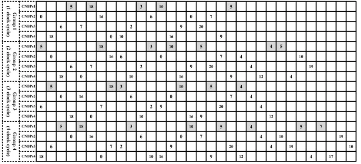
그림 1. 672 비트, rate-1/2 QC-LDPC 코드의 4 블록-병렬 계층 복호구조
Fig. 1. Four block-parallel layered decoding scheme of 672-bit, rate-1/2 QC-LDPC code.
DVB-S2, IEEE 802.16e and IEEE 802.11n. In addition, millimeter wave (mmWave) Wireless Personal Area Networks (WPANs) described by the IEEE 802.15.3c Working Group[1] are considering LDPC codes as the preferred choice for forward error correction (FEC).
Recently, many studies have been accomplished aimed at simplification of the VLSI implementation of the related decoders which are called “Architecture -Aware LDPC codes” or “Block-LDPC codes”. Based on these design approaches, quasi-cycle (QC) LDPC codes have received significant attention due to their efficient hardware implementations. Furthermore, QC-LDPC codes can provide comparable error-correction performance compared with random LDPC codes.
With the increasing demand for high-data-rate wireless application, an overlapped decoding architecture and a layered decoding architecture are popular for high-throughput LDPC decoding architectures using QC-LDPC codes. An overlapped decoding architecture[2],[3] based on the partially parallel architectures using a belief-propagation decoding (BP) algorithm, where the message updating computations in the check node unit (CNU) and the variable node unit (VNU) are partially overlapped,
can increase the decoding throughput by maximizing the hardware utilization efficiency without any performance degradation.
Compared with the overlapped two-phase decoding scheme, a layered decoding algorithm and architecture have been proposed in order to achieve a faster convergence[4∼5]. Generally, the layered decoding algorithm is the horizontal layered decoding algorithm which is favorable for the Min-Sum algorithm. In [5], the layered decoding algorithm offers 2x throughput and significant memory advantages, compared with the BP algorithm.
In this paper, we propose a four block-parallel layered QC-LDPC decoder architecture for a 672-bit, rate-1/2 QC-LDPC code in IEEE 802.15.3c standard.
The proposed architecture enables the concurrent processing of four block rows of the H matrix and the replacement of all of the crossbar-based interconnect network with a fixed wire network.
Furthermore, two-stage pipelining technique is employed to achieve high clock speed and high data throughput.
The rest of this paper is organized as follows.
Section II describes the design issues related to the QC-LDPC decoder. Section III describes the proposed
QC-LDPC decoder architecture. In Section IV, the implementation and comparison are presented. Then, conclusions are presented in Section V.
Ⅱ. Design Issue Related to QC-LDPC Decoder for WPAN Applications
1. Difficulties of Parallel and Pipelining Techniques for High-Throughput Layered Decoders.
The layered decoding algorithm which is a modified version of the BP algorithm can reduce the average number of iterations using an intermediate check-node (or variable-node) message values by almost 50% compared with the BP algorithm.
Therefore, it offers 2× throughput without performance degradation. However, due to the data dependency between consecutive rows in the layered decoding, the parallel and pipelining techniques cannot
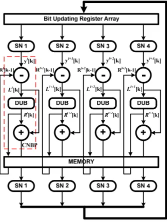
그림 2. 4 블록-병렬 계층 복호 회로의 데이터흐름 Fig. 2. Dataflow of four block-parallel layered decoding
scheme.
be applied directly. The QC-LDPC codes which are composed of sub-matrices enable to the implementation of a block parallel layered decoding architecture. In the QC-LDPC codes, the consecutive rows in a block row of H matrix (a layer) operate independently because the column weight of each sub-matrix is at the most 1. In other words, instead of one row, one block row which is composed of z rows can be updated simultaneously at 1 clock cycle.
However, the layered decoder needs to be extended to provide higher parallelism as the demand beyond 1 Gbps throughput increases, but there is no layered decoder architecture in which two or more block rows can be updated simultaneously at only 1 clock cycle. The decoding scheme involving a 672-bit rate-1/2 QC-LDPC code in the IEEE 802.15.3c standard is shown in Fig. 1. The check node-based processors (CNBPs), which consist of z CNBPs[6], perform computation of a block row and each CNBP performs the computation of a row.
Fortunately, for the H matrix of our selected LDPC code, the column weight of four block rows is at the most 1 without the need for reordering of the H matrix. Thus, four block rows can be computed simultaneously by four CNBPs at only 1 clock cycle.
Using this scheme, a four block-parallel layered decoding architecture (4-BPLDA), which consists of four CNBPs, can be designed for the proper trade-off between the decoding throughput and the hardware complexity.
In order to achieve higher throughput, the pipelining technique can be used. However, for the layered decoding algorithm, the computations of the CNBPs shown in Fig. 2 are sequentially performed and the newly updated variable messages, which are fed into the bit updating register array, are used immediately with the next layer. If the pipelining technique is used amongst three consecutive computations without an effective method, the next layer must wait for the number of the pipelining stage until the newly updated variable messages is
passed to it. To solve this problem, the approximate layered decoding scheme for two-stage pipelining[6] is adopted. This method minimizes the bit error rate (BER) performance loss caused by pipelining.
2. High Routing Complexity Due to Increased Parallelism
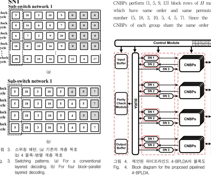
By increasing the parallelism of the H matrix, the main issue in the hardware implementation is how to reduce the routing complexity. A conventional layered decoding architecture needs two switch networks (SNs) for shuffling and reshuffling messages. A SN consists of eight sub-switch networks in which a sub-switch network is used for switching z messages in a sub-matrix. The switching pattern of a conventional layered decoding is shown in Fig. 3
(a)
(b)
그림 3. 스위칭 패턴. (a) 기존의 계층 복호 (b) 4 블록-병렬 계층 복호
Fig. 3. Switching patterns. (a) For a conventional layered decoding. (b) For four block-parallel layered decoding.
(a), where the values in the shaded blocks are meaningless values. Each sub-switch network in the SN1 performs four different cyclic shifts and needs to change the cyclic shift in each clock cycle. This requirement can result in the use of the crossbar-based interconnect network[8] which increases the hardware and routing complexity.
Especially, the proposed 4-BPLDA needs 12 SNs with pipelining technique.
If all of the SNs in the proposed 4-BPLDA are implemented with the crossbar-based interconnect network, the hardware and routing complexity become much higher. As illustrated in Fig. 1, for the proposed four block-parallel layered decoding scheme, first CNBPs performs {l, l+4, l+8, l+12} block rows of the H matrix which have only the same order and same permutation number. For example, the first CNBPs perform {1, 5, 9, 13} block rows of H matrix which have same order and same permutation number {5, 18, 3, 10, 5, 4, 5, 7}. Since the first CNBPs of each group share the same order and
그림 4. 제안된 파이프라인드 4-BPLDA의 블록도 Fig. 4. Block diagram for the proposed pipelined
4-BPLDA.
permutation number as shown in Fig. 3 (b), the first sub-switch network in the SN1 of first CNBPs always performs 5 right cyclic shifts to the z messages. For this reason, the proposed fixed wire network is used for all the SNs of the 4-BPLDA and this network is able to maximize the H matrix utilization efficiency of our selected LDPC code.
Ⅲ. Proposed QC-LDPC Decoder Architecture
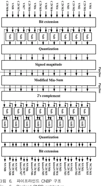
In this section, the proposed 4-BPLDA for a 672-bit, rate-1/2 QC-LDPC code is proposed, as shown in Fig. 4. Based on the approximate layered decoding algorithm, the overall decoder architecture was designed. The 4-BPLDA mainly consists of a memory block for storing messages, CNBPs for processing intermediate messages, SNs for routing messages, a bit updating register array (BURA) for storing intermediate messages, a parity check module and a decoder control module. The CNBP has two pipelining stages, in which the decoding update block (DUB) has been designed with the modified Min-Sum algorithm.
1. Four-Block Parallel Layered Decoding Scheme
The approximate layered decoding algorithm[7] with the modified Min-Sum algorithm[9] can be expressed as follows:
] 1 [ ] [ ]
[ '1 '
' k = y−− k −R k−
Llv vl p cvl (1)
}) ] [ { min ( ] [ ]
[ 1
' ), ( 1
' 1
' k S k L k
R ln
v n c N n l
cv l
cv
−
≠
∈
−
− =α ⋅ ⋅ (2)
∏≠
∈
−
− =
' ), (
1 1
'[ ] ( [ ])
v n c N n
l n l
cv k sign L k
S (3)
] [ ]
1 [ ]
[ ]
[ '1 ' '
' k y k R k R k
ylv−p = vl−−p − cvl−p − + cvl−p (4)
where ′ in (4) denotes the C2V message conveyed from the check node c of (l-p)-th layer to
variable node v', which is the same value as
′ in (1) before two clock cycles, and
′ in (4) denotes the latest variable message connected to the check node c of (l-p)-th layer. To update the variable message ′ , the result of (1) is re-computed by using ′ ′ in (4). Although the part ′ ′ in (4) is a redundant computation, it enables two-stage pipelining with a slight BER performance loss.
2. Overall Architecture of the Proposed Decoder
The decoding process of the proposed decoder architecture can be carried out as follows:
1) Initialization: The incoming soft messages are shifted into the BURA from the input buffer. The BURA is composed of 32 registers and a register is mapped to a sub-block of the H matrix. The first layer is decoding, when all of the registers are filled up.
2) Switch network 1, 3: For notational simplicity, we omit eight registered MUX blocks, where four registered MUX blocks are between the BURA and each SN1, whilst the other registered MUX blocks are between the BURA and each SN3. Four registered MUX blocks simultaneously load the required messages into each SN 1 from the BURA.
Following that process, each SN1 rotates the input messages by the amount of the related permutations.
Then, the messages are fed into each of the CNBPs.
The other four registered MUX blocks load the latest variable messages stored in the BURA into each SN3. Following that, each SN3 rotates the latest variable in each SN3. After that stage, each SN3 rotates the latest variable messages by the amount of the related permutations. Then, the latest variable messages are fed into each CNBP. Unlike the other inputs in the CNBPs, the latest variable messages are not passed to the two pipeline stages, as shown in
Fig. 6. This result means that the latest variable messages are not loaded into the SN3 until 3 clock cycles. Also, the SN3 at (i+2) clock cycles performs the same operation as does the SN1 at i clock cycles.
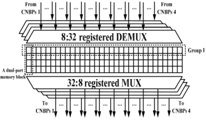
3) CNBPs operation: The variable messages and the C2V messages from the memory are loaded into each CNBP. The CNBPs computes (1) and (2) for the newly updated C2V messages. For the computation shown in (4), the latest variable messages, the C2V messages and the newly updated C2V messages are used in the CNBPs. The newly updated C2V messages are stored back in the memory and the newly updated variable messages corresponding to the computation results of (4) are delivered to the SN2. Four CNBPs can share a memory, which is shown in Fig. 5. The memory is composed of 32 dual-port memory banks and a group stores newly updated C2V messages for the four block rows of the H matrix. In order to avoid memory conflicts, read and write spaces in each dual-port memory bank are differentiated. As a result, read and write operations are concurrently performed. The newly updated C2V messages by each CNBP are delivered to each registered DEMUX block, as shown in Fig. 5. Then four registered DEMUX blocks simultaneously load the newly updated C2V messages into the same group of the related dual-port memory banks. In the same way, four registered MUX blocks simultaneously load the related C2V messages stored in the next group for computation of each CNBPs.
그림 5. 32-듀얼-포트 메모리 블록 Fig. 5. 32-dual-port memory blocks.
4) Switch network 2: The newly updated variable messages are delivered to each SN2. Following this delivery, each SN2 re-rotates the input messages by the amount of the registered DEMUX blocks between the BURA and each SN2. Finally, the previous messages are replaced with the newly updated variable messages in BURA by the four registered DEMUX blocks.
5) Parity check: For parity checking at the end of every layer, the early termination strategy[10] is used in our design. The early termination strategy is flexible with respect to different signal-to-noise ratios (SNRs) and it reduces the hardware complexity compared with a typical parity check equation corresponding to In×HT=0, where In={in1,in2,…,inM}
denotes the estimated information bits. In the hardware implementation, the early termination strategy is easily employed by the use of M flip-flops, M XOR logic-gates and one M-input OR gate.
3. Pipelined CNBP Architecture
Fig. 6 shows the pipelined CNBP architecture using the approximate layered decoding algorithm. A CNBP, which performs a row of H matrix, computes equations (1), (2) and (4). Since the sequential computations in the CNBP have a long computation delay, a CNBP needs to be split into two pipeline stages in order to reduce the critical path delay and to improve the clock speed. The dashed-lines in the CNBP denote the two-stage pipelining. The variable messages and the C2V messages extend the bits in the extension block and perform the computation shown in (1). The signed magnitude, modified Min-Sum and the 2’s complement block perform the functions defined in (2). The newly updated C2V messages, which are the outputs of the 2’s complement block, are fed to the quantization block.
The quantization block can prevent the newly updated C2V messages from overflow. Finally, the newly updated C2V messages are stored back in the
그림 6. 파이프라인드 CNBP 구조 Fig. 6. Pipelined CNBP architecture.
memory. The newly updated C2V messages, C2V messages and the latest variable messages rotated by the SN3 are used to perform the computation defined in (4). Finally, the newly updated variable messages are fed into the quantization block and then are delivered to the SN2.
IV. Performance Comparison
The proposed 4-BPLDA was modeled in Verilog HDL and then simulated so as to verify the functionality using a test pattern generated from a C simulator. After complete verification of the design functionality, the 4-BPLDA was synthesized using
그림 7. N=672, rate-1/2 불규칙적인 QC-LDPC 코드의 비트 에러율
Fig. 7. Bit error rate for N=672, rate-1/2 irregular QC-LDPC code.
appropriate time and area constraints. Both simulation and synthesis steps were carried out using a SYNOPSYS design tool and 90-nm CMOS technology optimized for a 1.08V supply voltage. Fig.
7 shows the BER performance of the QC-LDPC code using the layed decoding for α = 1, 0.875, 0.75 through C modeling. As α decreases from 1, the BER performance significantly improves. The standard layered decoding with the Min-Sum (α=1) was about 0.3 dB performance loss compared with the standard layered decoding with the modified Min-Sum (α
=0.875). It should be noted that the performance of the standard layered decoding with the modified Min-Sum (α=0.75) is the best with low SNR (< 2.5 dB). However, it causes a high error flow, as shown in Fig. 7. For this reason, a α=0.875 and a (q, f) = (6, 2) quantization scheme is adopted, where q and f are the total bit size of the intrinsic message and the number of fractional bits, respectively. 8 bits are used for representing the values of the total bit size of the extrinsic message. The parameter p in equations (1) and (4) is set to 2 and the maximum iteration number is set to 12. The throughput rate of the proposed decoder can be calculated according to
×
× (5)
×
× ×
(6)
Table 1 shows performance comparison results for the 4-BPLDA with and without pipelining. The proposed pipelined 4-BPLDA operates at a maximum frequency of 290 MHz. The data decoding throughput is estimated to be approximately 3.9 Gbps using a maximum of 12 decoding iterations, as shown in
Design 4-BPLDA
with pipelining
4-BPLDA without pipelining
Block size 672 672
Iterations 12 8
CMOS tech. 90 nm 90 nm
Max. clock freq(MHz) 290 120
Throughput(G/bs) 3.9 2.52
Gate counts(gates) 794K 611K
표 1 파이프라이닝과 파이프라이닝 하지 않은
4-BPLDA의 성능 비교
Table 1. Performance comparison of 4-BPLDA with pipelining and without pipelining.
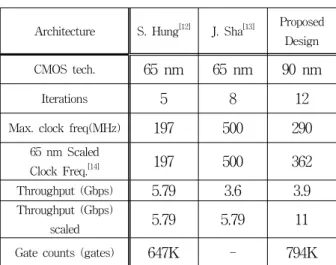
Architecture S. Hung[12] J. Sha[13] Proposed Design CMOS tech. 65 nm 65 nm 90 nm
Iterations 5 8 12
Max. clock freq(MHz) 197 500 290
65 nm Scaled
Clock Freq.[14] 197 500 362
Throughput (Gbps) 5.79 3.6 3.9
Throughput (Gbps)
scaled 5.79 5.79 11
Gate counts (gates) 647K - 794K 표 2. WPAN 시스템을 위한 QC-LDPC 복호기의 성
능 비교
Table 2. Performance comparison of QC-LDPC decoders for WPAN applications.
equation (5) and (6). For the 4-BPLDA without pipelining, the maximum clock frequency is 120 MHz and the data decoding throughput is also estimated to be approximately 2.52 Gbps using a maximum of 8 decoding iterations. Although the approximate layered decoding has a small performance loss (< 0.15 dB) with a quantization scheme rather than with standard layered decoding, the proposed decoding technique can achieve a much higher throughput by increasing the clock frequency. Throughput shown in Table 1 and 2 depict worst case where total number of iterations is 12. But the layered decoding algorithm used in this paper converges much faster at high SNRs. So, even more throughput enhancement is possible if we use less number of decoding iterations at high SNRs. We have observed that it is possible to terminate the decoding at iterations 9 and 10 for SNRs in excess of 2.5 dB and 3.0 dB respectively to achieve the same BER performance shown in Fig. 7.
Early termination strategy described in Section III can terminate the decoding at any iteration number.
This gives a throughput enhancement in excess of 5 Gbps.
The proposed decoder design is compared with the existing QC-LDPC decoders, as shown in Table 2.
The LDPC decoder architectures given in [12] shows good throughput result but the throughput calculated for 5 iterations. Lesser number of iterations means higher throughput and worse BER that is why BER of [12] shows worse results than our results. To make a fair compassion, we have also calculated the throughput of proposed design using 5 iterations and with the frequency scaled to 65 nm technology[14]. The throughput is effectively doubled and show 11 Gbps for 5 iterations. Thus, the proposed LDPC decoder architecture can be a powerful LDPC scheme for high throughput multi-gigabit WPAN applications.
V. Conclusions
This paper has presented a high-throughput
pipelined 4-BPLDA of QC-LDPC code for high-rate WPAN applications. The proposed architecture enables a high throughput and a very low decoding latency. The routing complexity was reduced significantly by replacement of a crossbar-based interconnect network with a fixed wire network for SN. Hence, the proposed decoder architecture has a high throughput, low routing complexity and very low decoding latency. The proposed architecture is expected to be incorporated in next-generation multi-gigabit WPAN applications.
References
[1] “Wireless Medium Access Control (MAC) and Physical Layer (PHY) Specifications for High Rate Wireless Personal Area Networks (WPANs): Amendment 2: Millimeter-wave based Alternative Physical Layer Extension,” 2008.
IEEE P802.15.3c/D04
[2] L. Liu and C.-J. R. Shi, “Sliced message passing: High throughput over- lapped decoding of high-rate low-density parity-check codes,”
IEEE Trans. Circuits Syst. I, Reg. Papers, vol.
55, no. 11, pp. 3697-3710, Nov. 2008.
[3] 나영헌, 신경욱, “IEEE 802.11n용 다중모드 Layered LDPC 복호기,” 대한전자공학회 논문지, 제48권 SD편, 제 11호, 18-26쪽, 2011년 11월.
[4] M. Mansour and N. Shanbhag, “High-throughput LDPC decoders,” IEEE Trans. VLSI Syst., vol.
11, no. 6, pp. 976-996, Dec. 2003.
[5] D. E. Hocevar, “A reduced complexity decoder architecture via layered decoding of LDPC codes,” IEEE Workshop on Signal Processing Systems (SiPS), pp. 107-112, Oct. 2004.
[6] S. Kim, G. E. Sobelman, and H. Lee, “Flexible LDPC decoder architecture for high-throughput applications,” in Proc. IEEE Asia Pacific Conf.
Circuits Syst. (APCCAS), Macao, China, pp.
45-48, Nov. 2008.
[7] Z. Cui, Z. Wang, and Y. Liu, “High-throughput layered LDPC decoding architecture,” IEEE Trans. VLSI Syst., vol. 17, no. 4, pp. 582-587, April 2009.
[8] S. Kim, G. E. Sobelman, and H. Lee, “A Reduced-Complexity Architecture for LDPC Layered Decoding Schemes,” IEEE Trans. VLSI
Syst., vol. 19, no. 6, pp. 1099-1103, June 2011.
[9] S. Zhao, Z. Farhad, “On implementation of Min-Sum algorithm and its modifications for decoding Low-Density Parity-Check (LDPC) codes,” IEEE Trans. Commun., vol. 53, no. 4, pp.
549-554, Aug. 2005.
[10] X.-Y. Shih, C.-Z. Zhan, C.-H. Lin, and A.-Y.
Wu, “An 8.29 mm2 52mW Multi-Mode LDPC Decoder Design for Mobile WiMAX System in 0.13μm CMOS Process,” IEEE J. Solid-State Circuits, vol. 43, no. 3, pp. 672-683, March 2008.
[11] S. H. Kang and I. C. Park, “Loosely coupled memory-based decoding architecture for low density parity check codes,” IEEE Trans.
Circuits Syst. I, vol. 53, no. 5, pp. 1045-1056, May 2006.
[12] S. Hung, S. Yen, C. Chen, H. Chnag, S. Jou, C.
Lee, “A 5.7Gbps row-based layered scheduling LDPC decoder for IEEE 802.15.3c applications”, 2010 IEEE Asian Solid State Circuits Conference (A-SSCC), Nov. 2010.
[13] J. Sha, J. Lin, Z. Wang, L. Li, M. Gao, “LDPC decoder design for high rate wireless personal area networks”, IEEE Trans. Consumer Electronics. vol. 55, no. 2, pp. 455-460, May 2009.
[14] Z. Cui, Z. Wang, and X. Wang, “Reduced- complexity column-layered decoding and implementation for LDPC codes,” IET Commun., vol. 5, no.15, pp. 2177-2186, Oct. 2011.
저 자 소 개 이 한 호 (정회원)
1993년 충북대학교 전자공학과 학 사 졸업
1996년 Univ. of Minnesota 전기 컴퓨터공학 석사 졸업 2000년 Univ. of Minnesota 전기
컴퓨터공학 박사 졸업 2000년∼2002년 Member of Technical Staff,
Lucent Technologies (Bell Labs.), USA.
2002년∼2004년 Assistant Prof. Dept. of Electrical and Computer Engineering, Univ. of Connecticut, USA.
2004년~현재 인하대학교 정보통신공학부 교수
<주관심분야 : 통신용 VLSI 및 SoC설계>
Sabooh Ajaz (학생회원)
2006년 NED University of Engg.
&Tech. Karachi, 전자공학과 학사 졸업 2010년 University of
Wollongong, Australia, Electrical Computer and Telecom Engineering 석사 졸업
2011년~현재 인하대학교 정보공학과 박사 재학
<주관심분야 : 통신용 VLSI 및 SoC설계>