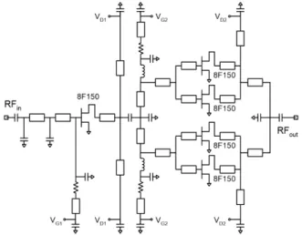
A 20 W GaN-based Power Amplifier MMIC for X-band Radar Applications
7
0
0
전체 글
(2)
(3)
(4)
(5)
(6)
(7)
수치


관련 문서
The paper examines the incentives of power generating companies (GENCOs) for efficient fuel procurement for power generation under the Cost-Based Generation
Based on the results, this study concluded that competitive power of construction business in uncertain management environment lies in human resources rather
The reduction of power series ( , m→ ∞) to polynomials (m is finite) is a great advantage.. because then we have solutions for all x,
Ä White LED (Sold-State Lighting) Ä High Power (RF) Devices (Military).. Nichia’s Blue LED with GaN
¾ Q s and r are used to “steal” some base current away from Q 1 when the output is accidentally shorted to ground, preventing when the output is accidentally shorted
¾ Efficiency is defined as the average power delivered to the load divided by the power drawn from the supply:. Emitter Follower
Also, an intermodulation distortion is formed due to the nonlinear characteristics of power amplifier near the saturation region when more than two
“Evaluation of R&D investments in wind power in Korea using real option.” Renewable and Sustainable Energy Reviews. "Real Option Valuation of a Wind Power Project Based
