A Method for Reducing the Number of Metal Layers for Embedded LSI Package
Daisuke Ohshima
1,†, Kentaro Mori
2, Yoshiki Nakashima
2, Katsumi Kikuchi
2and Shintaro Yamamichi
21
System Jisso Research Laboratories, NEC Corporation
2
Device Platforms Research Laboratories, NEC Corporation 1120 Shimokuzawa, Sagamihara 229-1198, Japan (Received October 13, 2010 : Accepted November 17, 2010)
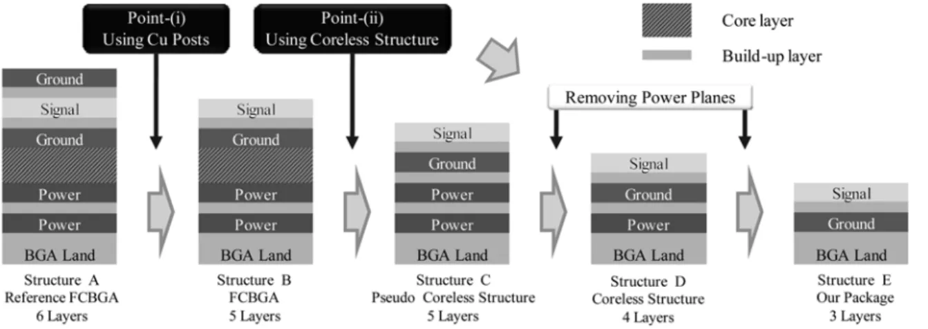
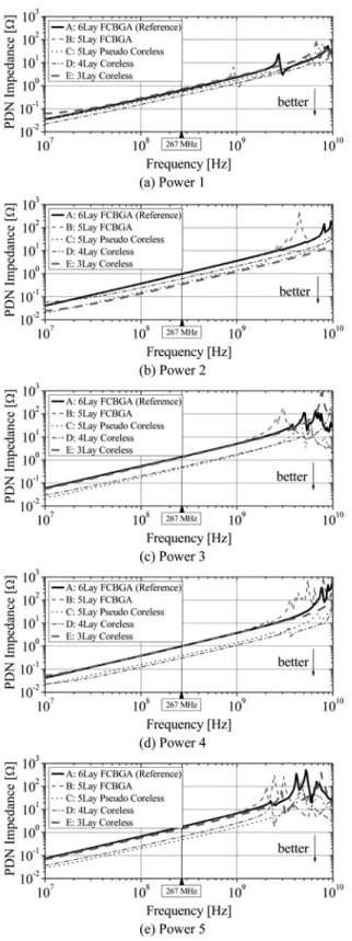
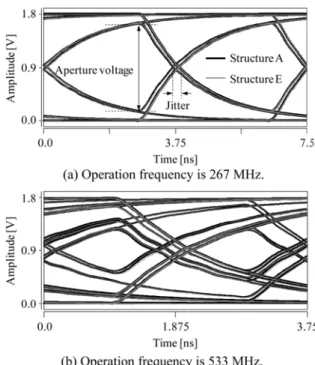
Abstract: We have successfully demonstrated a high-pin-count and thin embedded-LSI package to realize next generation's mobile terminals. The following three design key points were applied: (i) Using Cu posts, (ii) Using the coreless structure, (iii) Using a Cu plate as the ground plane. In order to quantitatively determine the contribution of the three points, the five-stage process for reducing the number of metal layers is described by means of the electrical simulation. The point-(i) and (ii) are effective from the viewpoint of the power integrity (PI); that is, these points play important roles in reducing the number of metal layers, and especially the point-(ii) contributes at least twice as the point- (i). The point-(iii) is not effective in the PI, but has a few effects on the signal integrity (SI). For reducing the number of metal layers, we should, at first, pay attention whether the PI characteristics fulfill the specification, and then we should confirm the SI characteristics.
Keywords: Embedded-LSI packaging, power integrity characteristics, signal integrity characteristics, next generation mobile terminal
1. Introduction
Continuous demands for small form factor and multi functions for mobile terminals will definitely open a new market for personal devices. They will be realized with small and thin housing, just like fashionable mobile phones, and high-performance for multi-media contents, just like laptop PCs. As the early stage of next generation's mobile terminals, smart phones and netbook PCs have been emerged as examples. These kinds of terminals appear to be complement between mobile phones and laptop PCs.
From the viewpoint for the components of these terminals, the LSI package for the next generation's mobile terminals should be large size and compatible to high-pin- count LSIs, compared to the current devices. Therefore, it is important for the LSI package to be shrank, and we successfully developed a thin embedded LSI package and demonstrated its normal operation.
1-2)In order to realize our embedded LSI package, the electrical design technology for reducing the number of metal layers contributed greatly, as well as the fabrication process developments.
As shown in our previous study
1-2), we described the following three design points to realize this package:
(i) Using Cu posts
(ii) Using the coreless structure
(iii) Using a Cu plate as the ground plane
This paper describes the five-stage design process for reducing the number of metal layers for embedded package, in detail. We analyzed how much each design point contributes to the electrical characteristics.
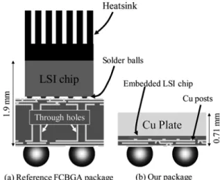
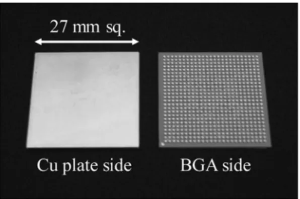
2. Package Structures
First, we describe the features of our LSI package by comparing with a reference FCBGA package. Figure 1
†