1. 서 론
실리콘 (Si) 은 충분한 매장량과 낮은 유해성으로 인해 태양광 산업에서 가장 각광받고 있는 물질로 전체 태양광 시장의 90%
이상을 차지하고 있다. 이중 multi-crystalline silicon (mc-Si) 을 이용한 태양전지는 전체 실리콘 태양광 시장의 70%를 차지하 고 있지만, mc-Si이 갖는 다수의 grain boundary와 상부 textured surface의 낮은 광흡수율로 인하여 single-crystalline silicon (sc-Si) 태양전지에 비해 ~2% 낮은 광전환 효율을 보인다. mc-Si 의 경우, sc-Si과 달리 isotropic alkali etching을 이용한 마이크 로 사이즈의 피라미드 texturing이 불가하기 때문에 광반사율이 높게 나타난다. 이로 인하여, 표면 texturing과 반사방지막 코팅 을 포함한 경우, sc-Si 태양전지의 광반사율은 350~1050 nm 파 장대 영역에서 ~5%정도 이지만 mc-Si 태양전지의 광반사율은 10%이상을 보인다1-3).
이러한 단점을 극복하기 위하여, 최근 레이저 식각법4), reactive
ion 식각법5), 무전해 식각법6)등을 이용하여 광반사율이 0%에 가까운 nano-textured black multi-crystalline silicon (Bmc-Si) 이 각광받고 있다. 이러한 nano-textured Bmc-Si은 높은 광흡수 율을 갖지만, 그에 따른 surface recombination center의 증가로 실질적인 태양전지 효율 증가에 크게 영향을 미치지 못한다. 또 한 실리콘 표면에 고종횡비의 구조체가 형성되므로 균일한 전 극 형성에도 어려움이 있다7,8).
이에 본 연구에서는, 값비싼 진공장비 없이 wet-hood 안에서 공정이 진행되는 무전해 식각법과 추가적인 alkali-based 식각 법을 통하여 mc-Si 표면에 나노사이즈의 피라미드 구조체를 제 작하였다. 이를 통하여 균일한 상부전극 형성이 가능하며, mc-Si 태양전지의 단점인 낮은 광흡수율도 높일 수 있는 나노사 이즈 피라미드 구조체 최적화 연구를 실행하였다.
2. 실 험
2.1 실리콘 웨이퍼 saw damage 제거 공정
표면의 나노사이즈 피라미드 구조는 wet-based 공정으로 Ag nano particle을 이용한 무전해 식각법과 KOH를 이용한 추가적
Current Photovoltaic Research 5(1) 25-27 (2017) pISSN 2288-3274
DOI:https://doi.org/10.21218/CPR.2017.5.1.025 eISSN 2508-125X
고효율 다결정 실리콘 태양전지 제작을 위한 나노크기의 피라미드 텍스쳐 제작
허 종1,2)ㆍ박민준1)ㆍ지홍섭1)ㆍ김진혁2)ㆍ정채환1)*
1)한국생산기술연구원 광에너지융합그룹, 광주광역시, 61012
2)전남대학교 신소재공학과, 광주광역시, 61186
Nanoscale Pyramid Texture for High Efficiency Multi-Crystalline Silicon Solar Cells
Jong Heo1,2) ․ Min-Joon Park1) ․ Hong sub Jee1) ․ Jin Hyeok Kim2) ․ Chaehwan Jeong1)*
1)
Applied Optics and Energy Research Group, Korea Institute of Industrial Technology, Gwangju 61012, Korea
2)
Department of Material Science and Engineering, Chonnam National University, Gwangju 61186, Korea
ABSTRACT: Nanoscale textured black silicon has attracted intensive attention due to its great potential as applications in multi- crystalline silicon-based solar cells. It absorbs sunlight over a broad range of wavelengths but introduces large recombination centers, non-uniform doping into cell. In this study, we present a metal-assisted chemical etching technique plus alkaline etching process to fabricate nanoscale pyramid structures with optimized condition. To make the structures, silver nanoparticles-loaded mc-Si wafer was submerged into H
2O
2/HF solution first for nanohole texturing the wafer and textured wafer etched again with KOH solution for making nanoscale pyramid structures. The average reflectivity (350-1050 nm) is about 8.42% with anti-reflection coating.
Key words: Multi-crystalline silicon, Solar cell, Nano-pyramid, Surface texturing, Photovoltaic
*Corresponding author: [email protected]
Received November, 21, 2016; Revised December, 21, 2016;
Accepted December, 23, 2016
ⓒ 2017 by Korea Photovoltaic Society
This is an Open Access article distributed under the terms of the Creative Commons Attribution Non-Commercial License (http://creativecommons.org/licenses/by-nc/3.0)
which permits unrestricted non-commercial use, distribution, and reproduction in any medium, provided the original work is properly cited.
25
J. Heo et al. / Current Photovoltaic Research5(1) 25-27 (2017) 26
인 alkali-based 식각법을 통하여 제조되었다. 200 μm 두께의 mc-Si 웨이퍼(ρ=0.5-3.0 Ω · cm)를 40×40 mm2크기로 잘라 기 판을 준비하였다. 준비된 기판을 CH3COOH 와 HF, HNO3를 10:3:6의 비율과 10:6:6의 비율로 혼합한 용액에 1분 담지하여 웨이퍼 표면의 saw damage를 제거한 후, 1:10의 비율로 희석된 HF 수용액에 담지하여 표면에 형성된 native oxide를 제거한다.
2.2 나노 피라미드 구조 제작 및 반사방지막 코팅 공정 saw damage가 제거된 실리콘 기판을 10 mM의 AgNO3와 4.8 M의 HF 용액에 10초간 담지하여 Fig. 1(a)에서처럼 표면에 Ag particle을 형성하였으며, 곧바로 4.8 M의 HF와 0.5 M의 H2O2용액에 1분을 담지하여 Fig. 1(b)와 같이 식각하여 nanohole 구조를 우선 제작하였다. 무전해 식각법을 통한 nanohole 제작 공정 후, 남아있는 Ag particle은 HNO3용액에 3분간 담지하여 제거하였다. nanohole 구조가 형성된 기판을 80°C의 0.01 M KOH 수용액에 4, 5, 6분간 각각 담지하여 나노사이즈의 피라미 드 구조체를 Fig. 1(c)와 같이 형성하였다.
입사광의 흡수율을 극대화하기 위하여 plasma enhanced chemical vapor deposition (PE-CVD) 을 이용하여 반사방지막 층을 증착하였다. 본 실험에 적용된 반사방지막은 80 nm 두께의 SiNX:H 박막으로 2.1의 굴절률을 가지며, 이는 최적화된 조건 으로 보고되어 있다9).
2.3 특성분석
제작된 나노 피라미드 구조는 field emission scanning electron microscope (FE-SEM, FEI)을 이용하여 분석하였다. 또한, 제작 된 나노 피라미드의 광특성을 분석하기 위하여 Perkin Elmer Lambda 750 UV/Vis/NIR spectrophotometer를 적분구와 함께 이용하여 측정하였다.
3. 결과 및 고찰
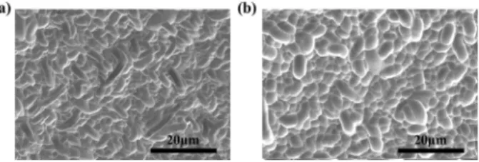
Fig. 2는 mc-Si 웨이퍼의 saw damage를 제거 한 후의 표면을 SEM 분석을 통해 나타내었다. Fig. 2(a)는 CH3COOH 와 HF, HNO3를 10:3:6의 비율로 혼합한 용액에 담지 하였으며, Fig.
2(b)는 10:6:6의 비율로 혼합한 용액에 담지하였다. 위의 비교를 통하여 HF 용액의 비율을 높일수록 표면의 거칠기가 거칠어지 는 것을 알 수 있다.
Fig. 3은 각각의 조건에서 saw damage가 제거된 웨이퍼의 광 반사율을 측정한 데이터이다. 광 반사율 데이터에서 알 수 있듯 이 표면의 거칠기가 큰 CH3COOH:HF:HNO3 = 10:3:6의 비율 로 혼합한 용액에 담지한 웨이퍼의 반사율은 350-1050 nm 파장 영역에서 28.1%를 보인 반면, 상대적으로 거칠기가 작은 10:6:6 의 비율의 용액에 담지 되었던 웨이퍼의 광반사율은 32.8%를 보 였다.
Fig. 4은 무전해 식각법을 통하여 nanohole 구조체 제작 후, 추가적인 alkali-based 식각 시간을 조절하여 나노사이즈 피라 미드 구조체를 제작한 SEM 분석 자료를 보여준다. Nanohole 구 조체가 형성되어 있는 기판에 추가적인 alkali-based 식각을 5분 동안 진행하였을 경우 가장 최적화된 나노사이즈 피라미드 구 조체를 형성 할 수 있었다 (Fig. 4(b)). 반면에 Fig. 4(a)에서 보이 듯이 alkali-based 식각 시간이 4분일 경우, 기판에 형성되어 있 던 nanohole 구조체가 남아 있는 것을 확인 할 수 있다. 이는 추가 적인 alkali-based 식각 시간이 부족하여 발생된 현상이며, 이와 는 반대로 Fig. 4(c)와 같이 6분 동안 alkali-based 식각을 진행한 경우 형성된 나노사이즈 피라미드의 형태가 과도한 식각으로 인해 희미해지는 것을 확인할 수 있다.
Fig. 1. Schematics of three steps preparing nanoscale pyramid texture
Fig. 2. SEM surface image of CH
3COOH/HF/HNO
3acid etching.
The ratio of mixture is (a) 10:3:6 and (b) 10:6:6
Fig. 3. Reflectivity of acid-etched mc-Si subatrate
J. Heo et al. / Current Photovoltaic Research5(1) 25-27 (2017) 27
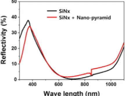
Fig. 5은 나노사이즈 피라미드의 유무에 따른 광학적 특성 변 화를 분석한 데이터이다. 나노사이즈 피라미드를 제작하지 않 은 기판과 제작한 기판에 각각 PE-CVD 공정을 이용하여 80 nm 두께의 반사방지막 코팅을 진행 한 후 반사율을 측정하였다. 그 결과, 나노사이즈 피라미드를 제작하지 않은 기판의 경우 350~1050 nm 파장대 영역에서 9.90%의 광반사율을 보였지만, 나노사이즈 피라미드를 제작한 경우 8.42%의 광반사율을 보였 다. 특히 나노사이즈 피라미드 제작에 따른 650-1050 nm 파장 영역에서의 광흡수율 향상이 눈에 띄었다. 나노사이즈 피라미 드 제작에 따른 광반사율(3.30%)이 그렇지 않은 샘플(5.81%)에 비하여 약 43%의 광반사율 저감효과를 갖는 것으로 분석되었 다. 이를 통하여 나노사이즈 피라미드가 장파장 영역에서의 광 반사율을 획기적으로 줄일 수 있다는 것을 알 수 있다.
4. 결 론
본 연구에서는 공정비용이 저렴한 무전해 식각법과 추가적
인 alkali-based 식각법을 이용하여 mc-Si 기판에 나노크기의 피 라미드 구조체를 성공적으로 제작하였다. 나노크기의 피라미드 구조체는 장파장 영역에서의 광반사율을 크게 감소시키는 것으 로 분석되었다. 이는 기존의 mc-Si 태양전지의 단점인 높은 광 반사율을 효율적으로 감소 시킬 수 있고, 상부전극 제작도 nano-textured Bmc-Si에 비하여 용이하기 때문에 mc-Si 태양전 지의 효율 향상에 크게 기여할 것으로 판단된다.
Acknowledgements
본 연구는 2016년도 산업통상자원부의 재원으로 한국에너 지기술평가원(KETEP)의 지원(No.20143020010860)과 또한 한국생산기술연구원 기관고유사업(E0160065, E0160038)을 통해 수행한 연구 과제입니다.
References