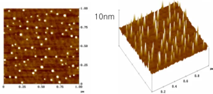
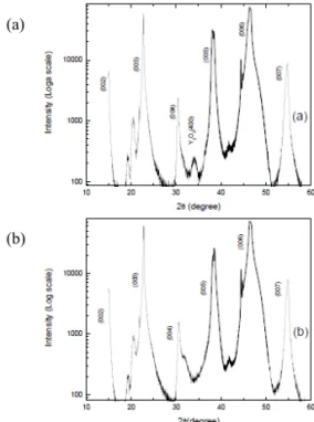
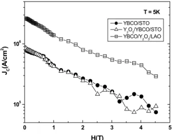
Effect of $Y_2O_3$ Nanoparticles on Critical Current Density of $YBa_2Cu_3O_{7-x}$ Thin Films
5
0
0
전체 글
(2)
(3)
(4)
(5)
수치
관련 문서
In a statement to Kuwait News Agency (KUNA) on the sidelines of a meeting of the Arab Parliament's Foreign Affairs Political and National Security
The meeting was attended by Assistant Foreign Minister for GCC Affairs, Ambassador, Nasser Al-Muzayyen, and Deputy Assistant Foreign Minister for the Office of the
“ Sheikh Nasser has a written message from HH the Amir, Sheikh Sabah Al-Ahmad Al-Jaber Al-Sabah to the Chinese President, Chi Gen Beng related to enhancing mutual
On his part, CEO of Express Roads Authority, Saud Al-Naqqi said that the heavy rains of the previous day led to clogging parts of the express
Kuwait will celebrate on Sunday the fourth anniversary of the UN honoring and proclamation of His Highness the Amir, Sheikh Sabah Al-Ahmad Al-Jaber Al-Sabah as
• 이명의 치료에 대한 매커니즘과 디지털 음향 기술에 대한 상업적으로의 급속한 발전으로 인해 치료 옵션은 증가했 지만, 선택 가이드 라인은 거의 없음.. •
The proposal of the cell theory as the birth of contemporary cell biology Microscopic studies of plant tissues by Schleiden and of animal tissues by Microscopic studies of
It considers the energy use of the different components that are involved in the distribution and viewing of video content: data centres and content delivery networks
