PHYSICAL REVIEWA VOLUME 50, NUMBER 4 OCTOBER 1994
Electro-optic
measurement
of
the electric-field distributions
in
coplanar-electrode
poled polymers
J.
W.WUDepartment
of
Physics, Ewha Womans University, Seoul 12075-0, South KoreaT.
Wada andH.
SasabeFrontier Research Program, The Institute
of
Physical and Chemical Research (RIKEN), Wako, Saitama 35101-,Japan (Received 9March 1994)Electric-field distributions incoplanar-electrode configurations are studied experimentally through the hnear electro-optic (EO) measurements in poled EO polymers. Thermoplastic poling ofan isotropic guest-host polyimide system was employed to investigate the electrostatic factors determining the field distribution inside the EO polymer. Electrostatic analysis ofthe field distribution shows that the intro-duction ofanew boundary condition formed bythe polymer surface isnecessary toaccount forfield dis-tributions measured by the linear EOefFect.
PACSnumber(s): 42.65.Vh, 41.20.Cv,42.70.Nq, 78.20.Jq
Polymeric materials received wide attention as electro-optic (EO)materials for their high processability and compatibility with current microelectronic tech-niques as well as for the intrinsic high-bandwidth response
of
organic molecules[1,
2].
EO
eff'ect, oneof
the second-order nonlinear optical processes, can exist in ma-terials lacking the centrosymmetry. InEO
polymers, the centrosymmetryof
polymer thin films isremoved by a dc electric-field polingto
achievea
macroscopic polar align-mentof
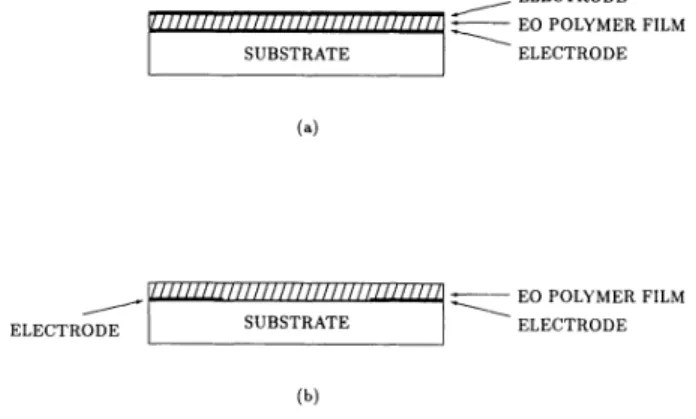
nonlinear optical chromophores. In thin-film samples, two configurationsof
electrodes are commonly adopted for the electric-field poling, parallel and coplanar (seeFig.
1). In the parallel-plate configuration,EO
poly-mer is sandwiched between two thin electrode plates on topof
a substrate (glass or silicon). In the coplanar-electrode structure, on the other hand, two thin separate electrodes with anarrow gap in between them are depos-ited on topof
the substrate, and thenEO
polymer film is spin coated. Two electrode configurations seemto
be equivalent as far as the dc electric poling andEO
mea-surements are concerned. However, detailed distribu-tionsof
the electric field inside polymer thin films are quite different.For
aparallel-electrode configuration, the electric-field distribution is almost uniform inside the po-lymer film between the top and bottom electrodes, be-cause the sizeof
electrodes is larger than the polymer thin-film thickness. In coplanar-electrode configurations, the film covers both electrodes and the dc poling andEO
effect measuring fields pass through and above the film,
making the electric-field distribution complicated. Ther-modynamic alignment
of
nonlinear optical chromophores between two electrodes follows electric-field lines which are not uniform across the gap. Even with this complica-tion, itis importantto
know the electric-field distribution in coplanar electrodes. When a practicalEO
device is designed for light modulations, coplanar-electrode design has merit asfar as processability is concerned, comparedto
parallel-plate electrode design.It
removes at least one or two stepsof
the metallization process for poling and modulation operation. In additionto
the practical reason, it is an interesting physics problem relatedto
the electrostatic boundary-value problem. Since thedielec-tric constant
of
polymer films is larger than thatof
the air, the electric-field lines have different shapes for different thicknessesof
thin films. Furthermore, the coplanar-electrode configuration withEO
polymers is foundto
be useful ror the electro-optic samplingof
high-speed signal transmissions in integrated circuits[3]
and also for the high-frequency light modulator[4].
In this paper, the electric-field distribution in the coplanar-electrode configuration is examined experimentally by preparing (electric-field poling) thin-film samples and measuringEO
effect. Theoretical analysisof
electrostat-ics with appropriate boundary conditions is compared with the experimental measurement and we find that there isagood agreement.In electrostatics, the electric-field distribution is ob-tained from the electrostatic potential. The electrostatic potential satisfies the Laplace equation in the absence
of
free charges. In this case, the field distribution is deter-mined solely from the boundary conditions.
For
two electrodes witha
finite potential difference, theelectric-field distribution is given in an elementary way.
It
isim-ELECTRODE //////////////////////////I I////// —
EOPOLYMER FILM
SUBSTRATE ELECTRODE
II I III I IIIIIIIIIIIIIIIIIII IIII II II = EOPOLYMER FILM
ELECTRODE SUBSTRATE ELECTRODE
(b)
FIG.
1.Two electrode configurations commonly adopted forEOpolymer films. EOpolymer is sandwiched between the top and the bottom electrodes in the parallel-plate electrode configuration (a),while EOpolymer is positioned on top of
co-planar electrodes with a narrow gap on substrate in the coplanar-electrode configuration (b).
3542
BRIEF
REPORTS 50 I J P p r+ w ~ a ~ ay$08
C NI
0 0.6 VI
LLJ E ~0.4 C Cl th A C V &0.2 I a ] -0.4 -0.2 0 0.2 0.4Horizontal Position inside the Gap (arb. units)
FKJ. 2. Computer-simulated plot of electric-field lines in coplanar-electrode configuration. x axis (abscissa) and y axis (ordinate) are equally scaled. Coplanar electrodes (not shown here) are placed on the left (x
= —
1.0}
and right (x=+1.
0)bottom. The dielectric constant eofpolymer thin film istaken as 3.4 [6]. The position of image charge is on the mirror-reflected point ofthe electrodes with respect to the polymer thin-film top surface, plane ofy
=+
1.0. That is, in this partic-ular example the film thickness ishalfofthe electrode gap size. The magnitude ofthe image charge is(e—
1}7'(e+1}.
portant, however, to note that the presence
of
the poly-mer film itself distorts the field lines due tothe introduc-tionof
anew boundary condition. Dielectric constantsof
polymer films being different from that
of
the air, the presenceof
a film on topof
a conductor (electrodes)pro-vides another boundary condition for the Laplace equa-tion. One way to solve the boundary-value problem like this is to introduce image charges. The image-charge method is very useful for the geometrically symmetric electrodes, which isthe case for coplanar electrodes. The position and size
of
the image charges depend on the thickness and the dielectric constantof
the polymer film[5].
Figure 2 shows the computer plottingof
the simulat-ed electric-field distribution for a thick polymer film when the proper image charge and the dielectric constantof
the polymer 61m are taken into account. Field strength gradually decreases as the vertical distance from the substrate increases. Field components along the sub-strate, responsible for theEO
effect in the coplanar-electrode configuration, also are not uniform across the gap. These variations will lead to a changeof EO
effects forfilms with different thicknesses.To
study the electric-field distribution experimentally from EO measurement, we employed a guest-hostpo-lyimide system. Since we are interested in the field distri-bution, we should be careful in selecting a model system to get rid
of
effects other than electrostatics. Structural anisotropy inherent to polymer films and chargeconcen-tration near electrodes, for example, may distort the electric-field distribution.
To
minimize the structural an-isotropy we chose the LQ2200compound (Hitachi Chem-icalCo.
)as the host polyimide system, which is known to possess an isotropic structure (optically and dielectrically)[6].
Furthermore, the guest-host polyimide systemshould have a suScient thermal stability
of
EO response at room temperatures after poling to study the fielddistribution
[7].
In this regard, a stilbene dye, 4-(dicyanomethylene)-2-methyl-6-(p-dimetylaminostyryl-4H-pyran} (DCM) molecule was chosen as guest non-linear optical molecules[9].
The DCM-LQ2200 guest-host system is knownto
possess a good thermal stabilityof
EO response in both through-imidization (thermoset-ting) and postinudization (thermoplastic) poling [7,8].
Compared with the through-imidization poling, the elec-tric current monitoring during poling shows that the pos-timidization (thermoplastic) poling near the glass transi-tion temperature minimizes the ion transport occurring during electric-field poling. Through-densification (ther-mosetting) poling
[10],
the other poling process possiblein polyimide systems, cannot be employed in the DCM-LQ2200 system due to the limited thermal stability
of
chemical bonds in
DCM
chromophores at thedensification temperatures exceeding
300'C.
Based on these considerations we chose an8%
solid solution DCM-LQ2200 guest-host polyimide as the materialsys-tem and we adopted the post-imidization (thermoplastic) poling for the electric-field poling.
It
is known that charge injection occurs in the coplanar-e1ectrode configuration when the dc poling field is applied at tem-peratures above the glass transition temperatureT
of
polymer
[11].
Sometimes the charge injection seems to lead to an apparent enhancementof EO
response[12].
In order to take careof
this charge injection problem, wekept the poling temperature at least
50'C
belowT
. Ac-cording to Valley etal.
[7],
T „appearing
in the VA'lliams-Landle-Ferry equation is in the rangeof 197'C
and
207'C
for the5%
and10%
guest contents inLQ2200 hosts.
T„
is usually about50'C
belowT
[13],
hence Ts will be about
250'C
for an8%
solid solution DCM-LQ2200 system. In fact, Ts, notT„,
is the tem-perature where the o.relaxationof
the polymer backbone occurs related tothe glass-rubber transition[14].
In preparing samples, 10-pm-gap coplanar chromium electrodes were patterned on top
of
fused quartz. The thicknessof
electrodes was around 5000 A, which ismuch srn.aller than the gap size
of
the coplanar elec-trodes. An8%
weight concentrationof
DCM in LQ2200 polyimide was prepared by overnight stirringof
DCM inLQ2200 polyamic acids. In order to study the
electric-field distribution vertical to the electrode plane, six sam-ples were prepared. Sample 1 has the EO polymer (DCM-LQ2200}
of
2pm thickness right on topof
the co-planar electrodes. After curing at250'C
for half an hour, itwas poled at the poling field strengthof
50V/pm at200'C
(about 50 C belowT
) for 1 min to minimize the charge injection. In sample 2,the base polymer with thicknessof
2 pm was spin coated on topof
coplanar electrodes and fully cured at300'C.
After that, the same FO polymer was spin coated on topof
the fully cured50
BRIEF
REPORTS 3543////////////////////////////////// = EOPOLYMER FILM BASEPOLYMER FILM (5)
ELECTRODE SUBSTRATE
BASEPOLYMER FILM(I)
ELECTRODE
FIG.
3. Film stack configuration ofsample 6 is shown. On top ofthe coplanar electrodes, five base polymer films (1)—(5) are spin coated and fully cured successively. Thereafter, EO poly-mer (top layer) is spin coated, cured, and poled.bare polymer, and cured again at
250'C
for half an hour. The poling was performed at the identical condition as sample1.
The same step was repeated for samples 3—
6; only the bare polymer thickness increased through suc-cessive spin coating and curing. Inthis way,EO
polymerof
the same thickness is positioned on topof
the elec-trodes with different vertical distance from the electrode, bare polymer films providing different spacings. Film stack configurationof
sample 6, for example, is shown inFig.
3.
EO
effect comes from the activeEO
polymer on the top layer, while the base polymer just sits thereto
provide vertical spacing between the electrode and the
EO
polymer, enabling usto
study the electric-field distri-bution.Since the
EO
signal has a good thermal stability at room temperature, it is easy to do theEO
measurement and compare the signals. The cross-polarizer lock-in technique was employedto
measure theEO
response [8,15].
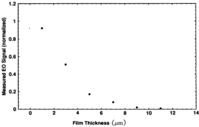
Figure4
shows the measuredEO
signal asa func-tionof
the film thickness. Nonlinear optical molecules residing inside theEO
polymer give rise to the measuredEO
signal, the magnitude providing i.nformation on thefield distributions in the top layer. That is, the
electric-field distribution determines both the orientational distri-bution function
of
guest molecules and the amountof
detected
EO
response. Different thickness samples willsample the field distribution at different vertical positions above the coplanar electrodes. As expected, the
EO
sig-nal decreases rapidly asthe film gets thicker.From the simple variation
of
the field distribution, two effects accumulate toresult inalarge difference in theEO
effect for films with different thicknesses. First, most im-portantly, the orientational distribution
of
nonlinear opti-cal molecules is different. The ratioof
the dipolar in-teraction energyto
the thermal energy,x
=pE
IkT,
varies inside the polymer film since the electric-field dis-tribution is not uniform. This means that one single dis-tribution function cannot describe the thermodynamic molecular alignment properly. In other words, the order parameter related to the achieved alignmentof
the non-linear optical molecules varies as a functionof
the verti-caldistance from the substrate as well as the lateral posi-tion inside the gap. The second effect, equally important, comes in when the linearEO
effect ismeasured. Changeof
the refractive index experienced by an optical light on the applicationof
a dc fieldEk,
which is the veryEO
effect, is described by an effective linear polarizability a';..
.
a',J( co;DI;0)=y~j~—q'( co;co,O)Ek.
—
For
a given field distributionof
the modulating electricHere both the poling field
E
and the measuring fieldE
have distorted field distribution as shown in
Fig.
2,whilethe optical field
E
passing through the film is not affected by field distortions. In estimating the distorted electric-field distribution from electrostatics the spatial variation across the 10-pm gap is averaged since the fo-cused beam spot size was not small enough aswell as our interest lies only on the vertical variationof EO
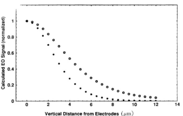
signal for different thickness thin films. Algebraic sumof
squaredvalues
of
horizontal componentsof
electric fields shown inFig.
2 provides the theoreticalEO
signal for oneEO
polymer film. In
Fig.
5,these calculated magnitudesof
EO
signal (closed circles) are drawn for EOpolymer thinfilms with different thickness base polymer. Also drawn are the algebraic sum
of
electric-field horizontal com-ponents (open circles), not the squared values, for com-parison.It
isobvious that the measuredEO
signals are in good agreement with the calculatedEO
signals. This suggests that distortionof
the electric fields in coplanar electrodes affects both the orientational distributionsof
chromophores and the EO measurements, resulting in quite reduced overall signals for thick films.
Second-harmonic generation (SHG) experiment will
1.2
1.
N CI E o 0.8 c ll C~06.
M0
LU ~0.4~ N CI ~o0. 2-0 . . a 0 8 10 FilmThickness (pm) 12 14FIG.
4. Measured EO signal using across-polarizer lock-in technique fordifferent thickness polymer films.field
Ek,
the amountof
refractive index change is not homogeneous across the gap between two electrodes. Distortionof
the electric-field results in the distortionof
the index changes accordingly. These two effects com-bine to give an overall variation on the EO effect for coplanar-electrode poled polymer thin films with different thicknesses. Since both the preparation (poling)
of
sam-ples and the measurementof EO
effect involve dc electricfields, the distortion effect is doubled, giving an enhanced effect in the end. The phase-shift difference bp=p~~
—
IIt~between the parallel and perpendicular components
of
a linearly polarized light along45'
relative to the polingfield direction can be expressed in terms
of
theEO
molec-ular hyperpolarizability P;Jk(—
co;co,O).For
a linearly shaped molecule likeDCM,
P333(—
co;co, O), the principal axis component along the molecular axis, is dominant. In the lowest order, b,Pis[16,
17]pEp
3544
BRIEF
REPORTS gp 1-N E o0.8. C ~06-CO 0 LLI 'g 0. 4-CP ~ 0. 2-0 1 ~ 0 ~ 0 0 0 0 0 0 0 0 0 ~ 0 ~ ~ Co.s.s. &a.0 0 0. a 6 8 10 12 14Vertical Distance fromElectrodes (pDI)
FIG.
5. Calculated EO signal (closed circles) for different thickness polymer films. The magnitude decreases rapidly as the film thickness increases. Calculated electrostatic fields along the substrate plane (open circles) are shown for compar-ison.separate out the poling effect and the
EO
coefBcient mea-surement effect. Fundamental light goes through the filmwithout being affected by the electric-field distribution
of
the electrode configuration forpoling. Macroscopic SHG polarization is
pE
p3 ~P333( 2copcopto)E3E3
kT
where only the poling field
E
not the measuring funda-mental optical fieldE3,
is distorted by the coplanar elec-trodes. Therefore SHG signals will decrease much moreslowly as the film thickness increases for the same coplanar-electrode poled sample. In other words, SHG signals will be the open circles
of
Fig.
5.In summary, electric-field distributions in coplanar-electrode configurations are investigated by measuring electro-optic response in a poled DCM-LQ2200 guest-host polyimide system. Electro-optic effects for films
with different thicknesses provide information on the field
distributions. Rapid decrease
of
the measured electro-optic response as the film thickness increases agrees wellwith the calculated electric-field distributions when prop-er boundary conditions are taken into account.
We gratefully thank
T.
Imai for providing the fused quartz cells with coplanar-electrode patterns.J.
W.W. would like to thankRIKEN
for the hospitality during the visit toRIKEN.
The workof
J.
W.W. was supportedby Korea Science and Engineering Foundations (Grant No. 931-0200-010-2)and Basic Science Research Institute Program, Ministry
of
Education, Republicof
Korea (Grant No. BSRI-94-2428).[1]See, for example, Nonlinear Optical Properties
of
Organic Materials IV, edited byK.
D.Singer, SPIE Conf. Proc. Vol. No. 1560(The International Society for Optical En-gineering, Bellingham, WA, 1991).[2]A.
F.
Garito,J.
W.Wu, G.F.
Lipscomb, andR.
Lytel, in Advanced Organic Solid State Materials, edited by L. Y. Chiang, P. Chaikin, and D. O. Cowan, MRS Symposia Proceedings No. 173 (Materials Research Society, Pitts-burgh, 1990), p. 467.[3]
J. I.
Thackara, D.M.Bloom, andB.
A.Auld, Appl. Phys.Lett. 59, 1159(1991).
[4] O. Solgaard,
F.
Ho,J.
I.
Thackara, and D. M. Bloom, Appl. Phys. Lett.61,2500 (1992).[5]
J.
D.Jackson, Classical Electrodynamics, 2nd ed. (Wiley, New York, 1975).[6] Hitachi Chemical Data Sheet, Hitachi Chemical Co.,Ltd. (1983).
[7]
J.
F.
Valley,J.
W.Wu, S.Ermer, M.Stiller,E.
S.Binkley,J.
T.Kenney, G.F.
Lipscomb, andR.
Lytel, Appl. Phys.Lett. 60, 160 (1992).
[8]
J.
W.Wu,J.
F.
Valley, S.Ermer, E. S.Binkley,J.
T.
Ken-ney, G.
F.
Lipscomb, andR.
Lytel, Appl. Phys. Lett. 58,225(1991).
[9] S.Ermer,
J.
F.
Valley,R.
Lytel, G.F.
Lipscomb, T.E
VanEck,and
R.
Lytel, Appl. Phys. Lett. 61,2272(1992). [10]J.
W.Wu, E. S.Binkley,J.
T.Kenney,R.
Lytel, and A.F.
Garito,
J.
Appl. Phys. 69, 7366(1991).[11]M.Stahelin, D.M.Burland, M. Ebert,
R.
D.Miller,B.
A.Smith,
R.
J.
Twieg, M.Volksen, and C.A. Walsh, Appl. Phys. Lett. 61,1626(1992).[12]S. Yitzchaik, G. Berkovic, and V. Krongauz,
J.
Appl. Phys. 70, 3949 (1991).[13]
J.
D. Ferry, Viscoelastic Properties ofPolymers, 3rd ed. (Wiley, New York, 1980).[14] N. G. McCrum, B.
E.
Read, and G. Williams, Anelastic and Dielectricsects
in Polymeric Solids (Wiley, NewYork, 1967).
[15]C. C. Teng and H. T.Man, Appl. Phys. Lett. 56, 1734
{1990).
[16]
K. D.
Singer, M. G.Kuzyk, andJ.
E.Sohn,J.
Opt. Soc.Am.