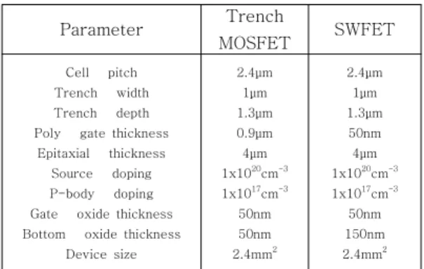
A Novel Structure for the Improved Switching Time of 50V Class Vertical Power MOSFET
8
0
0
전체 글
(2)
(3)
(4)
(5)
(6)
(7)
(8)
수치

+2
관련 문서
12 that절 내의 주어를 문장의 주어로 쓰고 that절 내의 동사를 to부정사로 써 서 수동태 문장을 만들 수 있다... 13 반복되는 the reason을 관계대명사 which로 바꿔주고
Our main contribution consists in the elevation of the DTW power of alignment from the lowest level (Class A, non-periodic time series) to the highest level (Class
Since every classical or virtual knot is equivalent to the unknot via a sequence of the extended Reidmeister moves together with the forbidden moves, illustrated in Section 2,
웹 표준을 지원하는 플랫폼에서 큰 수정없이 실행 가능함 패키징을 통해 다양한 기기를 위한 앱을 작성할 수 있음 네이티브 앱과
_____ culture appears to be attractive (도시의) to the
- In the future, the retail structure of power distribution may resemble the existing structure of the telephone industry.. Center for Power IT CENTER
- quadriceps tendon 이 슬개골 하연에서 tibial tuberocity에 부착.
The KBox A-150-BYT is connected by the Input power connector on the front panel to a DC power source via a DC power supply wiring; consisting of the Phoenix power
