제 2 회 첨단 사이언스 교육 허브 개발(EDISON) 나노물리 경진대회
Ab initio study of MoS 2 nanostructures
Janghwan Cha
Department of Physics and Graphene Research Institute, Sejong University, Seoul 143-747, Korea E-mail: [email protected]
The atomic and electronic properties of molybdenum disurfide (MoS2) nanostructures are investigated through density functional theory (DFT) calculations. We find that the band gap is indirect (about 1.79 eV) and direct (about 1.84 eV) in GGA for 2-dimensional MoS2 in our calculations. On the other hand, 1- dimensional armchair nanoribbons have semiconductor properties (band gap is about 0.11 ~0.28 eV), while 1-dimensional zigzag nanoribbons are metallic.
INTRODUCTION
The graphene has been expected to provide good performance due to its nano size effect and many interesting properties such as high electronic mobility and good transparency [1].
However, the zero band gap of graphene is main drawback for applications of electronic devices. The MoS
2has a band gap compared to the graphene. In this regard, it was suggested that MoS
2can be a complement to graphene for nano
device applications [2]. Furthermore, its layered structure can also be obtained by mechanical exfoliation method similar to the graphene.
SIMULATION METHODS
We have performed density functional theory (DFT) calculations to find atomic and electronic structure in generalized gradients approximation with SIESTA (Spanish Initiative for Electronic Simulations with Thousands of Atoms) program on the EDISON (EDucation-research Integration through Simulation On the Net) web site [3]. The model structure is that infinite 2-dimentional sheet and 1-dimentional nanoribbon structures are considered for MoS
2nanostructures, as shown in Figures 1 and 4. In the geometrical optimization, we use 3x3x1 and 5x1x1 k-points grid for 2- dimensional and 1-dimensional structures of MoS
2, respectively, in Monkhost-Pack scheme. In the band structure calculations, we use the ‘Post
Fig 1. (a) top and (b) side views of atomic structure of 2-dimensional MoS2. Light purple and yellow balls represent Mo and S atoms, respectively. Red arrows in (a) represent lattice vectors.
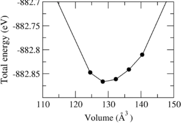
Fig 2. Total energy as a function of volume, which is used for calculation of lattice parameter.
15
214제 2 회 첨단 사이언스 교육 허브 개발(EDISON) 나노물리 경진대회
processing’ category in the EDISON web site for infinite 2-dimentional MoS
2, while 51x1x1 grid is used for 1-dimentional nanoribbon MoS
2in Monkhost-Pack scheme.
The 2-dimensional MoS
2sheet consists of 3 layered structures with 1 Mo atom and 2 S atoms in primitive unit cell. Figure 1 shows the optimized geometry of 2-dimensional MoS
2structure with hexagonal planar lattice similar to graphene. The 2-dimensional MoS
2sheet are placed on the xy-plane. The lattice vectors 𝑎⃗
1and 𝑎⃗
2have the same length with 120 degree interior angle. The vacuum region of about 10 Å is enough to neglect the inter layer interaction.
RESULTS
We have performed the total energy calculation to find the optimized unit-cell with changing lattice constant. As a result, we find that the optimized lattice parameter is 3.22 Å at each lattice vectors. Consequently, the cell volume is 128.39 Å
3(a
3= 15.0 Å), as shown in Figure 2.
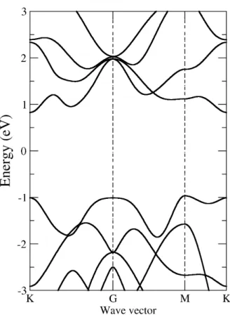
Now, we have calculated electronic band structure of 2-dimensional MoS
2using optimized lattice parameters, as mentioned above. In Figure 3,
Fig 3. Calculated band structure of 2-dimensional MoS2
Fig 4. (a) Zigzag and (b) armchair nanoribbon MoS2 structures.
16
215제 2 회 첨단 사이언스 교육 허브 개발(EDISON) 나노물리 경진대회
the band gap is indirect (about 1.79 eV) and direct (about 1.84 eV) for 2-dimensional MoS
2, respectively. The difference between valence band maximum and conduction band minimum at the point K is direct band gap. The indirect band gap is from G to K.
We have already calculated the band structure of 2-dimensional MoS
2using Vienna Ab-initio Simulation Package (VASP). The band structure is slightly different compared with the VASP results.
This difference may come from the insufficient input parameters in this calculations. In order to get more accurate results, we need to use sufficient input parameters.
We finally consider two types of MoS
2nanoribbon structures such as zigzag and armchair edge structures. Figures 4 (a) and (b) show the zigzag and armchair MoS
2nanoribbon structures, respectively.
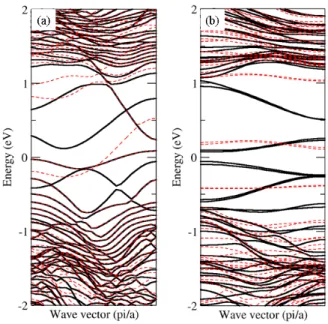
We find the band structure of zigzag and armchair nanoribbon MoS
2as shown in Figures 5 (a) and (b). In the width corresponding to N=13, we find that the band gap is 0.28 eV in the armchair nanoribbon. On the contrary, the zigzag nanoribbon shows metallic properties. In the band structures shown in Figure 5, spin-up and spin- down states are represented by black line and red
dotted lines. The band structures show that the nanoribbons have magnetic moments.
CONCLUSION
In summary, we investigated atomic and electronic structure of 1-dimensional and 2- dimensional MoS
2nanostructure. We found that the lattice constant of 2-dimensional MoS
2is 3.22 Å. We obtained electronic band structure of 2- dimensional MoS
2using optimized lattice parameters. The indirect band gap is about 1.79 eV and direct one is about 1.84 eV for 2-dimensional MoS
2. Also, we found that the zigzag MoS
2nanoribbons are metallic, while armchair MoS
2nanoribbons are semiconducting.
Thus, the MoS
2can be a good candidate for the nano devices.
ACKNOWLEDGEMENT
This research was supported by EDISON Program through the National Research Foundation of Korea (NRF) funded by the Ministry of Education, Science and Technology (2012M3C1A6035305).
R
EFERENCES[1] K. S. Novoselov et al., Science 306, 666 (2004).
[2] B. Radisavljevic et al., Nature Nanotechnology 6, 147 (2011).
[3] http://nano.edison.re.kr.
Fig 5. Electronic band structure of (a) zigzag and (b) armchair nanoribbon MoS2. Black lines and red dotted lines represent spin-up and spin-down states, respectively.