A Computational Study for Designing Electrical Contacts to MoS
2Monolayers
김휘수, 하현우
충남대학교 재료공학과, 대전광역시 서구 갈마 2동 1078 대한민국.
충남대학교 나노소재공학과, 대전광역시 유성구 궁동 414-6 대한민국.
e-mail: [email protected], [email protected]
ABSTRACTS
Graphene have renewed considerable interest in inorganic, two-dimensional materials for future electronics. However, graphene does not have a bandgap, it is limited to apply directly to transistors and logic devices. Hence, other layered materials such as molybdenum disulphide (MoS2) have been investigated to address this challenge.
Here, we find that the nature of contacts plays a more important role than the semiconductor itself.
In order to understand the nature of MoS2/metal contacts, we perform density functional theory electronic structure calculations based on linear combination of atomic for the geometry, bonding, binding energy, PDOS, LDOS and electronic structure. We choose Au as a contact metal because it is the most common contact metal. In this paper, we demonstrate MoS2/Au contacts have a more promising potential in flexible nanoelectronics than MoS2 itself.
INTRODUCTION
Layered materials such as graphene are of considerable interest as potential electronic materials for future electronics[1]. Furthermore, its unique electronic structure renders it as a promising active material for a number of applications including field-effect devices, sensors, and optical components[2]. However, due to the absence of band gap, the graphene-based field- effect transistors (FETs) have high OFF- currents[3]. Therefore, different approaches are proposed to induce a band gap in graphene, e.g., lateral confinement into nanoribbons. However, these approaches often result in a significant reduction of carrier mobility[4,5]. loss of
coherence[6], and increased OFF-current[7]
compared to graphene.
Here layered inorganic materials such as MoS2
are attracting significant amount of interest recently offering a suitable alternative due to their intrinsic bandgap[2]. Two-dimensional (2D) materials, such as molybdenum disulfide (MoS2) and other members of the transition metal dichalcogenides family, represents the ultimate scaling of material dimension in the vertical direction[8]. MoS2 is a typical example from the layered transition-metal dichalcogenide family of materials[9]. Metal dichalcogenide (MX2)(M = Mo and W; X =S, Se, and Te) belongs to the family of layered transition metal dichalcogenide, whose crystal structure is built up of X–M–X monolayers interacted through van der Waals forces[3]. A single molecular layer of MoS2
consists of a layer of Mo atoms sandwiched between two layers of sulfur atoms by covalent bonds. The strong intralayer covalent bonds confer MoS2 crystals excellent mechanical strength, thermal stability up to 1090°C in inert environment, and a surface free of dangling bonds[10,11].
Nanoelectronic devices built on 2D materials offer many benefits for further miniaturization beyond Moore’s Law[12,13] and as a high- mobility option in the emerging field of large-area and low-cost electronics that is currently dominated by low-mobility amorphous silicon[14]
and organic semiconductors[15,16]. 2D MoS2
exhibit a direct bandgap of 2 eV in contrast to an indirect bandgap of 1.8 eV for the bulk material[17]. Its 1.8 eV bandgap is advantageous over silicon for suppressing the source-to-drain tunneling at the scaling limit of transistors[18].
The planar nature and mechanical flexibility of 2D materials also make them excellent candidates for fabricating lightweight and roll able or foldable electronic systems on common commodities like paper, plastics, and textiles, as well as for constructing low-cost driving circuits for flat-panel display applications[19]. 2D materials are thus promising for improving the performance and enable new functionality of ubiquitous electronics and display technology, such as flexible radio frequency identification tags and enhanced integration of drivers and logic circuits into display backplanes[8].
In this paper, we perform density functional theory electronic structure calculations SW based on linear combination of atomic in Edison Nanophysics program for the geometry, bonding, binding energy, PDOS, LDOS and electronic structure to compare nature between MoS2 and MoS2 /metal contacts.
RESULT & DISCUSSION
In this work, we have used density functional theory electronic structure calculations SW based on the Linear Combination of Atomic Orbitals in the Edison Nanophysics program. These calculations were performed on the basis of density functional theory (DFT) as implemented in the SIESTA code. This program calculates electronic structure, force, stress tensor, electron density, geometry optimization, molecular dynamics, spin-polarized calculation, k-sampling of the Brillouin zone, local and orbital-projected density of states, COOP and COHP curves for chemical bonding analysis, dielectric polarization, phonons, and band structure. We have found a suitable MoS2/Au contacts model and studied electronic properties of MoS2 monolayer and MoS2/Au contacts model. The band structure, energy, PDOS, and LDOS of MoS2 monolayer and MoS2/Au contacts were calculated by the SIESTA program.
The each unit cell of the MoS2 and Au has each lattice constants of X-axis and Y-axis and was calculated using above the equation as shown in Figs. 1(a) and 1(b). Due to the fact that MoS₂ is monolayer, the unit cell of MoS2 can be extended.
Therefore, the lowest error number of between each unit cell of the MoS2 and Au is two, and at the sizes of each unit cell are 6.244Å ( at the X-
Fig. 1. Real space of MoS2 and Reciprocal space. (a) The unit cell of MoS2 monolayer, the lattice constant of each unit cell and burgers vector. (b) The equation for to find critical K- point.
axis ) and 10.815Å (at the Y–axis ) in the MoS₂, and 6.01Å ( at the X-axis ) and 10.41Å ( at the X- axis ) in the Au. Through these results data, we made structure files. We have used these structure files for geometry optimization in the Edison Nanophysics program using density functional theory electronic structure calculations SW based on the Linear Combination of Atomic Orbitals, and structure files was sampled by a 11 X 11 X 1 K-point grid. The reason why we used K-point test is to find a suitable unit cell for this experiment.
As a result, we found an unchanged value at 11 K- point grid, so we calculated this sampling at the 11X11X1 K-point grid as shown in Fig. 2.
Fig. 2. K-point test value. A most stable K-point grid value is 11X11X1
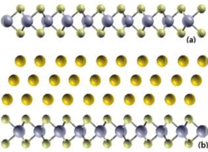
Fig. 3. Side view of the relaxed region (a) MoS2 and side view of the relaxed contact region at the interface between (b) MoS2 and Au (close-packed system)
Supercell geometry of the relaxed commen- surate contact region between MoS2 and the close- packed surfaces of Au is shown in Figs. 3(a) and 3(b). The monolayer MoS2 consists of a moly- bdenum monolayer sandwiched between two sulfur monolayers. Since monolayer MoS2 appears to fall short of its promising potential in flexible nanoelectronics, we expected that MoS₂/metal contacts will have more promising potential in flexible nanoelectronics. Therefore, we chose Au because it is the most common contact metal.
To characterize the contact bond strength, we define the binding energy E between the metal and the MoS2 layer as the total energy difference between the combined and the isolated systems and display our results in Fig. 4. Fig. 4(a) shows the relationship between initial bonding distance and bonding energy when MoS2 and Au are contacted.
The lowest energy was showed in the distance of 2.46674 Å . When Au is translated to x-axis, the lowest energy was showed in the distance of 1.4 Å as shown in Fig. 4(b). In the same way, When Au is translated to y-axis, the lowest energy was showed in the distance of 0.5 Å as shown in Fig.
4(c). Fig. 4(d) shows the final result of combination between Fig. 4(b) and Fig. 4(c). The lowest energy was showed in the distance of 2.51574 Å [min(E = 0.6153d6 - 12.747d5 + 109.3d4 - 496.75d3 + 1262.5d2 - 1700.7d - 6082.2) ≈
−7030.12 at d=2.51574]. As a result, we noticed that a considerably strong bonding of MoS2/Au contacts are showed in the distance is 2.51574 Å .
Fig. 4. (a) The relationship between initial bonding distance and bonding energy when MoS2 and Au are contacted. (b) Au is translated to x-axis. (c) Au is translated to y-axis. (d) Final combination with graph (b) and (c).
We have analyzed MoS2 band structure. As seen Fig. 5, we found that the energy band gap is 1.90 eV when electrons are excited from K-band to K-band. Moreover, we found that the energy band gap is 2.10 eV when electrons are excited from Γ-band to Q-band. Also, as shown in Fig. 5, Vbmax is 0.1 eV above at Γ-point, and Cbmin is 0.1 eV below at Q-point. Consequently, we noticed that MoS2 is a direct band semiconductor and has electronic properties of semiconductor.
Fig. 5. MoS2 band structure
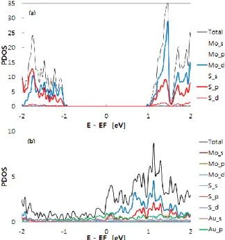
The density of states (DOS) of MoS2 at the Fermi level is shown in Fig. 6(a). Also, the Fig.
6(b) shows electron density of MoS2/Au contacts.
As seen by comparing Fig. 6(a) for MoS2 and Fig.
6(b) for MoS2/Au, Au as the contact metal modifies the electronic states near EF much more than MoS2. In the MoS2/Au contacts, the Fermi level is shifted upwards. This is much higher than in the MoS2 and causes an increase in the DOS at EF. Fig. 7 shows electronic structure at the interface between MoS2 and Au.
Fig. 6. (a) MoS2 (2H structure, monolayer) DOS.
(b) MoS2/Au contact DOS
Fig. 7. electronic structure at the interface(The cutting plane of normal direction to the z-axis).
CONCLUSION&SUMMURY
In conclusion, we performed density functional theory electronic structure calculations of MoS2
and MoS2/Au contacts based on linear combination of atomic in the Edison Nanophysics program to study the reason why monolayer molybdenum disulfide (MoS2) appears to fall short of its promising potential in flexible electronics according to recent experiments. We found that the nature of the contacts plays a more important role in these systems than the semiconductor itself. Our calculations for the geometry, bonding, DOS results, and electronic structure of the contact region suggest that the MoS2/Au contacts has better electronic properties rather than MoS2 itself.
As a result, MoS2/Au contacts compound can be a promising alternative to silicon-based, carbon-
based, and molecular electronics because of its structurally very flexibility, thus they are promising materials for future nanoelectronic device applications.
REFERENCES
[1] Yu, W.J., et al., Vertically stacked multi-heterostructures of layered materials for logic transistors and complementary inverters. Nat Mater, 2013. 12(3): p.
246-52.
[2] Pachauri, V., K. Kern, and K. Balasubramanian, Chemic- ally exfoliated large-area two-dimensional flakes of molybdenum disulfide for device applications. APL Materials, 2013. 1(3)
[3] Leitao, L., et al., Performance Limits of Monolayer Tran- sition Metal Dichalcogenide Transistors. Electron Devices, IEEE Transactions on, 2011. 58(9): p. 3042-3047.
[4] X. Li, X. Wang, L. Zhang, S. Lee, and H. Dai,
“Chemically derived, ultrasmooth graphene nanoribbon semi-conductors,” Science, vol. 319, no. 5867, p. 1229–
1232, Feb. 2008.
[5] L. Jiao, L. Zhang, X. Wang, G. Diankov, and H. Dai,
“Narrow graphene nanoribbons from carbon nanotubes,”
Nature, vol. 458, no. 7240, p. 877–880, Apr. 2009.
[6] F. Sols, F. Guinea, and A. H. C. Neto, “Coulomb blockade in grapheme nanoribbons,” Phys. Rev. Lett., vol. 99, no.
16, p. 166- 803, Oct. 2007.
[7] Y. Yoon and J. Guo, “Effect of edge roughness in graphene nanoribbon transistors,” Appl. Phys. Lett., vol.
91, no. 7, pp. 073103-1–073103-3, Aug. 2007.
[8] Wang, H., et al., Integrated circuits based on bilayer MoS(2) transistors. Nano Lett, 2012. 12(9): p. 4674-80.
[9] Radisavljevic, B., et al., Single-layer MoS2 transistors.
Nat Nanotechnol, 2011. 6(3): p. 147-50.
[10] Mak, K. F.; Lee, C.; Hone, J.; Shan, J.; Heinz, T. F.
Atomically Thin MoS2: A New Direct-Gap Semiconductor. Phys. Rev. Lett. 2010, 105, 136805.
[11] Spalvins, T. A review of recent advances in solid film lubrication. J. Vac. Sci. Technol., A 1987, 5, 212−219.
[12] Liu, L.; Kumar, S. B.; Ouyang, Y.; Guo, J. Performance limits of monolayer transition metal dichalcogenide transistors. IEEE Trans. Electron Devices 2011, 58, 3042−3047.
[13] Yoon, Y.; Ganapathi, K.; Salahuddin, S. How Good Can Monolayer MoS2 Transistors Be. Nano Lett. 2011, 11, 3768−3773.
[14] Street, R. A. Thin-Film Transistors. Adv. Mater. 2009, 21, 2007−2022.
[15] Forrest, S. R. The path to ubiquitous and low-cost organic electronic appliances on plastic. Nature 2004, 428, 911−918.
[16] Dimitrakopoulos, C. D.; Mascaro, D. J. Organic thin-film transistors: A review of recent advances. IBM J. Res.
Dev. 2001, 45, 11−27.
[17] J. K. Ellis, M. J. Lucero, and G. E. Scuseria, Appl. Phys.
Lett. 99, 261908 (2011).
[18] Wang, J.; Lundstrom, M. Does source-to-drain tunneling limit the ultimate scaling of MOSFETs? IEEE Tech. Dig.
IEDM 2002, 707−710.
[19] Bae, S.; et al. Roll-to-roll production of 30-in. graphene films for transparent electrodes. Nat. Nanotechnol. 2010, 5, 574−578.