제4회 첨단 사이언스 교육 허브 개발(EDISON) 나노물리 경진대회
Fig 2. jv.one.D그래프의 데이터 값
Fig 3. 도핑밀도를 바꾸기 전과 후(왼쪽이 바꾸기 전, 오른쪽이 바꾼후)
핑 밀도를 높게 해주었을 때 기본값에 비해 최 대전력 값이 올라가는 것을 볼 수 있다. 시뮬레 이션을 한 결과이고 그 밀도에 제한이 없었기에 100배나 높은 밀도를 줄 수 있었지만 실제 실험 에선 어느정도의 배율까지 가능할지는 잘 모르 겠으나 위의 시뮬레이션에서 알 수 있는 것은 도핑 밀도가 올라갈 시 보다 높은 최대 전력을 얻을수 있는 것을 알 수 있다. 그리고 최대전력 량이 높다해도 태양전지의 특성상 주변의 환경 태양전지가 받는 온도 등을 고려하여 보다 높은 전력을 보장받을 수 있게끔 개선방안이 필요 할 것 같다
CONCLUSION(또는 결론)
앞서 말한바와같이 시뮬레이션을 통해 구한 결 과이므로 실제 실험시 어떠한 변화가 있을진 잘
모르겠지만 확실한 것은 PN접합형 태양전지의 층 의 구성, 물질, 두께, 도핑밀도를 어떻게 조합하느 냐에 따라 얻을 수 있는 최대 전력이 바뀐다는 것 이다.
ACKNOWLEDGEMENT(또는 감사의 글)
제 4회 첨단 사이언스 교육 허브 개발 나노물리 경진대회를 통하여 평소 생소했던 학문을 보다 열 심히 배울 수 있었던 계기가 된점, 보다 관련 분야 에 관심을 가지게 된점을 감사히 생각하고있습니 다.
본 논문은 2015년도 정부(미래창조과학부)의 재 원으로 한국연구재단 첨단 사이언스·교육 허브 개 발 사업의 지원을 받아 수행된 연구임(No. NRF- 2012-M3C1A6035302)
REFERENCES(또는 참고문헌)
[1] http://blog.naver.com/padosori60 [2] http://cafe.naver.com/renewableenergy
75
제4회 첨단 사이언스 교육 허브 개발(EDISON) 나노물리 경진대회
Band Structure Engineering of Monolayer MoS
2by Surface Ligand Functionalization
Sang Yoon Lee and Sufyan Ramzan
School of Computer Science, Korea Advanced Institute of Science and Technology, Daejeon 305-701, Korea.
E-mail: [email protected]
Monolayer transition metal dicalcogenide (TMDC) materials are currently attracting extensive attention due to their distinctive electronic, transport, and optical properties. For example, monolayer MoS2 exhibits a direct band gap in the visible frequency range, which makes it an attractive candidate for the photocatalytic water splitting. For the photoelectrochemical water splitting, the appropriate band edge positions that overlap with the water redox potential are necessary. Similarly, appropriate band level alignments will be crucial for the light emitting diode and photovoltaic applications utlizing heterojunctions between two TMDC materials.
Carrying out first-principles calculations, we here investigate how the band edges of MoS2 can be adjusted by surface ligand functionalization. This study will provide useful information for the realization of ligand-based band engineering of monolayer MoS2 for various electronic, energy, and bio device applications.
INTRODUCTION
Monolayer transition metal dicalcogenide (TMDC) materials are currently attracting extensive attention.
Therefore, searching for and engineering efficient and TMDC is still a hot research topic. Recently, molybdenum disulfide (MoS2) has been extensively investigated. It is a layered hexagonal structure with a weak van der Waals interaction between individual sandwiched S-Mo-S layers. Bulk MoS2
has an indirect band gap of 1.2eV. Monolayer MoS2
(ML-MoS2) has a direct band gap of ~1.8eV, which is ideal for solar energy absorption. It was reported that the mobility of MoS2 can even be as large as 200cm2V-1s-1 at room temperature, although much lower values were obtained in other experiments which might originate from the existence of short- range surface defects. Moreover ML-MoS2 exhibits
high electrocatalytic activity and stability for the hydrogen evolution reaction (HER) in acidic environments. These advantages make ML-MoS2 a potential candidate for PEC water splitting. Similarly, appropriate band level alignments will be crucial for the light emitting diode and photovoltaic applications utlizing heterojunctions between two TMDC materials. In this article, I investigate how the band edges of MoS2 can be adjusted by surface ligand functionalization. My calculations show that useful information for the realization of ligand- based band engineering of ML-MoS2 for various electronic, energy, and bio device applications.
CALCULATION METHODS
Using the LCAODFTLab of EDISON Nanophysics, density functional theory (DFT) calculations were performed. All atomic positions and lattice consta nts were optimized until the Hellmann-Feynman 76
- 81 -
제4회 EDISON 사업 SW활용 경진대회 및 성과전시회 | 나노물리
367
제4회 첨단 사이언스 교육 허브 개발(EDISON) 나노물리 경진대회
(a)
(b)
(c)
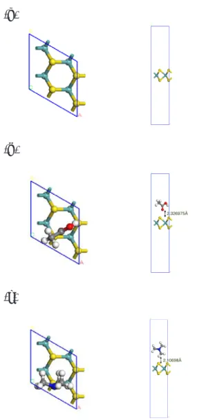
forces acting on each atom and the total energy c hange were less than 0.02eV and 0.0001eV, respec tively. The calculated lattice constants (a = b= 3.13 Å) of monolayer MoS2 are in fair agreement with the experimental values (a = b = 3.16 Å). ML- MoS2 was formed by cleaving form the surface of bulk MoS2 and incorporating a vacuum larger than 15 Å to ensure decoupling between neighboring slabs. As shown in Figure 1, a 2 X 2 super cell was used to select suitable ligands for surface functio nalization. The local density approximation (LDA) was implemented for the exchange correlation fun ctional. The Monkhorst-Pack k-
(d)
(e)
Fig. 33. Top and side views of (a) MoS2, (b) CA on a 2 X 2 ML-MoS2, (c) NMe3 on a 2 X 2 ML-MoS2, (d) PA on a 2 X 2 ML-MoS2 , (e) PO on 2 X 2 ML- MoS2
point was used for integration over the first Brillou
in zone. 10 X 10 X 1 k-
point meshes were adopted for geometry optimiz ation and electronic structure calculations, respecti vely.
RESULTS AND DISCUSSION
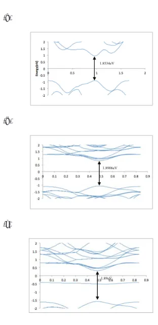
As shown in Figure 2(a), the calculated band gap of ML-MoS2 is 1.85 eV. Both VBM and CBM are composed mainly of Mo 4d and slightly of S 3p states, and the VBM is below the water oxidation level, whereas the CBM is located below the hydrogen redox potential. The calculation details of the average electrostatic potential and band edge positions of ML-MoS2 are given in the ESI. These results are all in good agreement with the experimental values. We first consider the surface 77
- 82 - 제4회 EDISON 사업 SW활용 경진대회 및 성과전시회 | 나노물리
368
제4회 첨단 사이언스 교육 허브 개발(EDISON) 나노물리 경진대회
(a)
(b)
(c)
forces acting on each atom and the total energy c hange were less than 0.02eV and 0.0001eV, respec tively. The calculated lattice constants (a = b= 3.13 Å) of monolayer MoS2 are in fair agreement with the experimental values (a = b = 3.16 Å). ML- MoS2 was formed by cleaving form the surface of bulk MoS2 and incorporating a vacuum larger than 15 Å to ensure decoupling between neighboring slabs. As shown in Figure 1, a 2 X 2 super cell was used to select suitable ligands for surface functio nalization. The local density approximation (LDA) was implemented for the exchange correlation fun ctional. The Monkhorst-Pack k-
(d)
(e)
Fig. 33. Top and side views of (a) MoS2, (b) CA on a 2 X 2 ML-MoS2, (c) NMe3 on a 2 X 2 ML-MoS2, (d) PA on a 2 X 2 ML-MoS2 , (e) PO on 2 X 2 ML- MoS2
point was used for integration over the first Brillou
in zone. 10 X 10 X 1 k-
point meshes were adopted for geometry optimiz ation and electronic structure calculations, respecti vely.
RESULTS AND DISCUSSION
As shown in Figure 2(a), the calculated band gap of ML-MoS2 is 1.85 eV. Both VBM and CBM are composed mainly of Mo 4d and slightly of S 3p states, and the VBM is below the water oxidation level, whereas the CBM is located below the hydrogen redox potential. The calculation details of the average electrostatic potential and band edge positions of ML-MoS2 are given in the ESI. These results are all in good agreement with the experimental values. We first consider the surface 77
제4회 첨단 사이언스 교육 허브 개발(EDISON) 나노물리 경진대회
(a)
(b)
(c)
functionalization of ML-MoS2 by various ligand groups, including CA, NMe3, PA, PO, to determine the most suitable surface functionalization ligand.
For CA, NMe3, PA, PO, no chemical bond is formed between the ligand and the surface and distance between them is about 2 Å. The band structure of MoS2 are displayed in Figure 2. Figure 3 displays the band edge positions of these ligand- funcionalized MoS2. As is clearly seen from the figure, no overlapping is observed between the ligands and MoS2, reflecting the weak interaction between ligand and MoS2. Interestingly, although
(d)
(e)
Fig. 2. Top and side views of (a) MoS2, (b) CA on a 2 X 2 ML- MoS2, (c) NMe3 on a 2 X 2 ML-MoS2, (d) PA on a 2 X 2 ML-MoS2, (e) PO on 2 X 2 ML-MoS2
Fig. 3. Calculated band edge positions of MoS2, CA, NMe3, PA and PO-functionalized MoS2
the charge transfer between the ligands and the s urface is very small, we observe charge transfer fr om MoS2 to CA and from PA and PO to MoS2.
CONCLUSION
In this paper, based on electronic structure calculations and analysis of band edge alignments, we have demonstrated that ML-MoS2
functionalized with ligand is an effective strategy 78
- 83 -
제4회 EDISON 사업 SW활용 경진대회 및 성과전시회 | 나노물리
369
제4회 첨단 사이언스 교육 허브 개발(EDISON) 나노물리 경진대회
for engineering the band gap of MoS2 to TMDC materials. I found that the ligand functionalization slightly influences the band gap of MoS2 but greatly affects its band edge positions.
ACKNOWLEDGEMENT
This research was supported by the EDISON Program through the National Research Foundation of Korea(NRF) funded by the Ministry of Science, ICT & Future Planning (No. NRF-2012- M3C1A6035302)
REFERENCES
[1] See ESI at http://www.rsc.org/nanoscale for futher results.
[2] Jing Pan, Zilu Wang, Qian Chen, Jingguo Hu, Jinlan Wang,
Nanoscale
., 2014, 6, 13565-13571.79
- 84 - 제4회 EDISON 사업 SW활용 경진대회 및 성과전시회 | 나노물리
370