한국표면공학회지 J. Kor. Inst. Surf. Eng.
Vol. 43, No. 4, 2010.
<연구논문>
Properties of Indium Doped Zinc Oxide Thin Films Deposited by RF Magnetron Sputtering
Joon Ho Bang
a, Se Hun Park
a, Sang Hyun Cho
b, Pung Keun Song
a*a
Department of Materials Science and Engineering, Pusan National University, Busan 609-735, Korea
b
Nano Convergence Practical Application Center, Daegu Technopark (Received August 29, 2010; revised August 29, 2010; accepted August 30, 2010)
Abstract
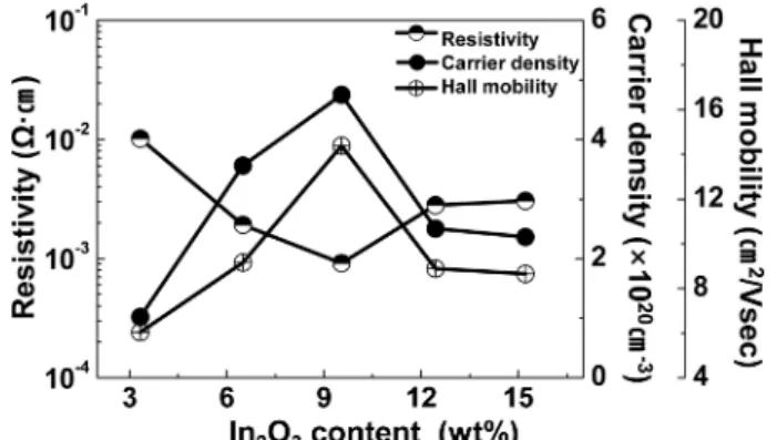
Indium doped zinc oxide films (ZIO) were deposited on non-alkali glass substrates by radio frequency (RF) magnetron sputtering at room temperature. The structural, electrical and optical properties of the ZIO films were investigated as a function of their In
2O
3content (3.33-15.22 wt%). The ZIO films deposited with an In
2O
3content of 9.54 wt% showed a relatively low resistivity of 9.13 ×10
−4Ωcm and a highly c-axis preferred orientation. The grain size and FWHM were mainly affected by the In
2O
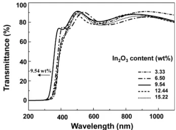
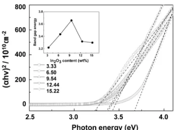
3content. The crystallinity and resistivity were enhanced with increasing grain size. The average transmittance of the ZIO films was over 85% in the visible region and their band gap varied from 3.22 to 3.66 eV depending on their doping ratio.
Keywords: ZnO, ZIO, TCO, RF magnetron sputtering
1. Introduction
Transparent conducting oxide (TCO) films with an optical transmittance exceeding 80% in the visible region and a low resistivity have been widely used in a variety of applications until now
1). Recently, TCO films have become the subject of intense investigation for use as transparent electrodes in optoelectric devices such as flat panel displays (FPDs), solar cells, infrared (IR) reflectors and organic light- emitting diodes (OLED). Most of the previous research on TCOs has been focused on indium tin oxide (ITO). However, TCO films based on zinc oxide (ZnO) have also received much attention, due to their advantages such as non toxicity, low cost and the relative abundance of this material
2,3). Furthermore, ZnO-based TCO films are more resistant to reductive hydrogen plasmas than In
2O
3-based films. TCO films can be prepared by a variety of techniques such as DC magnetron sputtering, RF magnetron sputtering, chemical vapor deposition (CVD), pulsed-laser deposition (PLD), molecular beam epitaxy (MBE)
and spray-pyrolysis
4). Normally, stoichiometric non- doped ZnO films present a high resistivity, due to their low carrier density. Therefore, Group III donor elements, such as Al, B, Ga and In, are added to improve the electrical properties of ZnO films. These high-valence metal elements can be regarded as the donor, which replaces the Zn atoms of the ZnO matrix
5). As a result, one electron is freed up to contribute to the electrical conductivity. Among the various zinc based TCOs, Al doped (AZO) and Ga doped ZnO (GZO) films have been extensively studied in recent years. Compared with AZO and GZO, there are few reports on In doped ZnO (ZIO).
2. Experimental
ZIO films were deposited on non-alkali glass (E2000) by RF (13.56 MHz) magnetron sputtering (Mirae Hi-tech Co., Ltd.) using high-density ceramic sintered ZIO targets with various In
2O
3contents (In
2O
3: 3.33, 6.50, 9.54, 12.44, 15.22 wt%; Samsung Corning Precision Glass Co., Ltd.). All of the deposition experiments were performed at room temperature (RT) under a pure argon atmosphere. The total gas
*