Vol. 71, No. 5, May 2021, pp. 457∼463 http://dx.doi.org/10.3938/NPSM.71.457
Deposition of Carbon Whiskers by Applying bias Voltage and Investigation of Their Field Emission Properties
Mincheol Kweon · Hong Jun Bark
∗Department of Material Physics, Dong-A University, Busan 49315, Korea (Received 20 October 2020 : revised 07 April 2021 : accepted 08 April 2021)
A carbon whisker-shaped thin film, similar to a carbon tube, was fabricated, instead of conventional diamond crystal particles, by applying a bias voltage to the silicon substrate.
The fabricated thin film was analyzed for shape and composition by using scanning electron microscopy and Raman spectroscopy. As the bias current was increased, the shape of the carbon whiskers tended to become thinner and longer, causing an increase in the field emission current. Additionally, an increase in the CH4 concentration and substrate temperature increased the whisker diameter. Moreover, an addition of NH3 increased the growth rate and caused the formation of sharp edges on the whiskers, resulting in a decreased operating voltage in field emission.
Keywords: Carbon whiskers, Field emission display, Thin film
I. INTRODUCTION
Spindt and co-workers fabricated and reported thin film field emission cathodes in 1976, leading to the devel- opment of field emission display (FED). Since then, the FED technology has been studied by several researchers for the application of FED devices as flat panel display devices or vacuum electronic devices because of their ad- vantages, such as low operating voltage, low power con- sumption, and the ability to reduce their thicknesses [1–
4]. Silicon or molybdenum, which has a high electron affinity, is used as the cathode material for field emission.
These cathodes are manufactured in the form of sharp tip arrays, using techniques, such as patterning and etch- ing in semiconductor processing, to facilitate field emis- sion even in a weak electric field. However, such tips are easily damaged owing to back sputtering by residual gas, and the electron emission performance is degraded because of the chemical reaction between the tip mate- rial and the residual gas, resulting in a stability problem [5]. To solve this problem, silicon carbide, diamond, or
∗E-mail: [email protected]
diamond-like carbon have been used as cathode materi- als [6–9]. Carbon-based materials have negative electron affinity; therefore, the field emission occurs easily, even with a weak electric field. Further, the carbon-based materials possess excellent mechanical properties, which reduce the tip damage caused by back sputtering, and excellent physical and chemical properties, such as chem- ical stability and high thermal conductivity. These fac- tors significantly improve the structural stability of the cathode [10–12]. In addition, efforts have been made to improve the field emission effect by adding dopants, such as boron and phosphorus, which considerably improved the field emission performance and cathode stability [13, 14]. However, for using diamond as an insulator in a field emission device, electrons must be easily discharged even when a low voltage is applied. Therefore, to facilitate the emission, we can either dope the fabricated device with impurities, such as nitrogen, or grow the device into a needle shape [15,16].
To solve this problem, Ren et al. devised a method in which a glass substrate, coated with nickel, was pre- treated with NH3or N2and then, a carbon tube was de- posited, using acetylene gas as the reaction gas, by main- taining the substrate temperature below 700 ◦C [17].
This is an Open Access article distributed under the terms of the Creative Commons Attribution Non-Commercial License (http://creativecommons.org/licenses/by-nc/3.0) which permits unrestricted non-commercial use, distribution, and reproduction in any medium, provided the original work is properly cited.
tion; therefore, they exhibit an improved field emission as compared to the diamonds by a factor of approximately – 10−4 [18]. Owing to these advantages, several stud- ies are being actively conducted to utilize carbon tubes as field emission devices [19]. In the formation of car- bon tubes, transition metals, such as nickel and cobalt, are deposited on the substrate. These transition metals form islands using catalyst gases, such as NH3 and N2, which can maintain continuous growth during the depo- sition process. These transition metals guide the carbon tube formation process, and therefore, their deposition is imperative for the pretreatment process. Here, one of the physical mechanisms is based on the bulk diffusion of carbon, dissolved in nickel, which can explain the low reactivity on noble metals as these metals do not dissolve carbon [20].
In general, different phenomena, such as promotion of nucleation, increase in the number of active ion species, and surface bombardment, are caused by the magnitude and direction of the applied voltage, type of reaction gas, and application time. Therefore, a bias voltage is ap- plied to improve the density and growth rate of the thin films. Additionally, in the semiconductor processing, a bias volt is used in the dry etching process to fabricate a substrate of the desired shape. Further, the fabrication of vertically aligned carbon tubes, by applying a negative bias voltage using a microwave device, has been studied as well [21]. However, the formation of a carbon whisker on a silicon substrate has not been studied to date.
Therefore, in this study, a carbon whisker-shaped thin film, such as a carbon tube, was fabricated on a silicon substrate, without depositing a transition metal, and an- alyzed using various effects of the bias voltage applied to the substrate. The shape and composition of the fab- ricated thin film was analyzed, using scanning electron microscopy (SEM) and Raman spectroscopy, to investi- gate its basic field emission characteristics, thereby as- certaining its application as a field emission device.
ple was placed) was controlled, by flowing cooling water inside the deposition chamber, and measured using a K- type thermocouple. For the substrate, a p-type silicon wafer (111) was cut into a 6 × 6 mm2 size, scratched with a diamond suspension of 0.1 µm diameter, followed by ultrasonication, first in acetone and then in alcohol, for 20 min. Next, the silicon substrate was etched in 10%
hydrogen fluoride solution for 5 min, dried with dry N2
(99.999%), and finally, mounted on the substrate holder.
First, the pressure in the vacuum chamber was reduced to 10−3 torr with a rotary pump, the main valve was closed, and hydrogen gas (99.999%) was injected into the chamber by controlling its inflow with a flow con- troller. The reaction pressure was maintained by a by- pass needle valve. The pressure in the vacuum chamber was measured with a manometer, and when it reached a set value, an alternating current was gradually (to main- tain the reaction temperature) applied to the filament.
To deposit a carbon tube-type carbon whisker, CH4 gas was introduced into the vacuum chamber, using a flow controller, and the bias current (Ib) was controlled under a filament temperature (Tf) of 1920◦C, substrate tem- perature (Ts) of 850◦C, pressure (P ) of 20 torr, and bias voltage (Vb) between – 500 V and + 35 V on the sub- strate, while maintaining the hydrocarbon (CH4) con- centration constant at 1%, for a deposition time (tdep) of 3 h.
To investigate the field emission characteristics of the deposited carbon whiskers, an indium tin oxide coated glass was used as the anode, and a glass fiber with a di- ameter of 230 µm was used as the spacer to maintain a certain distance from the sample. The sample was con- nected to the cathode, using carbon tape, and a direct current was applied to both ends of the anode and cath- ode, using a DC power supply. The experiment was per- formed at a pressure of 1× 10⁻⁵ torr, and the resulting field emission current was measured with an electrom- eter. The sample leakage current was measured in nA order at 1000 V in the device.
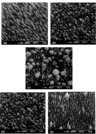
Fig. 1. SEM images of the carbon whiskers deposited by applying various bias currents (Ib) under the following conditions: Tf = 1920◦C, Ts = 850 ◦C, P = 20 torr, tdep = 3 h, and CH4 = 1%. (a) Ib = 0 mA, (b) Ib = – 100 mA, (c) Ib = – 300 mA, and (d) Ib = – 500 mA.
III. RESULTS AND DISCUSSIONS
1. Bias voltage effect
Figure 1 shows the SEM images of a thin film de- posited by varying the bias current from 0 to – 500 mA.
Using these, we can investigate the relationship between the bias current and morphology of the thin film. It was observed that as the bias current is increased, the length of the whisker is increased, and the diameter of the whisker tends to decrease. This change in the whisker dimensions occurs because the bonding of the deposited carbon particles is affected by the bias current. Thus, we can see that instead of growing diamonds, as shown in Fig. 1(a), the increase in the bias current enhances the formation of whisker-like carbon tubes on the silicon substrate, as shown in Fig. 1(b)–1(d). It seems that the edges of scratches on the silicon substrate, where the electric field is increased by the edge effect, act as nucle- ation sites for forming carbon whiskers at the nucleation stage. This is evidenced by the fact that we can hardly grow carbon whiskers on the polished substrate without scratches.
Raman spectroscopic analysis of the composition and crystal state of the particles show that only the sam- ple, grown without applying a bias current, exhibits a diamond characteristic peak in the Raman spectrum, as
Fig. 2. Raman spectra for depositions at (a) Ib = 0 mA, (b) Ib = – 100 mA, (c) Ib = – 300 mA, and (d) Ib = – 500 mA.
shown in Fig. 2(a). The Raman spectra of all the other samples show a gentle carbon characteristic peak in a wide area between 1400 cm−1 and 1600 cm−1, which in- dicates that carbon is present in an amorphous form in these samples. Therefore, when a bias current is not applied, diamond, with low density and growth rate, is deposited, as shown in Fig. 1(a); however, when a bias voltage is applied, carbon whiskers are grown, instead of diamond. From this observation, we can infer that CH4
does not form diamond on the silicon substrate, depend- ing on the bias current; instead, it forms whisker-like carbon tubes, depending on the strength of the applied electric field. In addition, it is thought that the length of the whisker is increased because the ionic species that are located at the selected positions of the substrate grow in the vertical direction, along which the electric field is strengthened by the continuously applied bias, rather than in the horizontal direction, according to the silicon substrate.
In this study, we investigated whether SUS, which is usually used as a substrate holder material formed by bias sputtering, exhibited characteristics of a transition metal or not. Therefore, to block the role of the tran- sition metal, the SUS 304 substrate holder was replaced with a carbon plate of 99.999% purity, and the other deposition parameters were tested under the same con- ditions, as before. It was found that carbon whiskers
Fig. 3. SEM images of carbon whisker deposited (a) on Si substrate without transition metal coating (deposition for 3 h) (b) Bias (2 h) + non Bias (1 h), (c) Bias (1 h) + non Bias (2 h) under the following conditions: Tf = 1920
◦C, Ts= 850◦C, P = 20 torr, Vb= – 270 V, Ib= – 300 mA, CH4= 1%), and (d) under the same aforementioned conditions except for the positive bias voltage (Vb = + 30 V) and current (Ib = + 300 mA).
were deposited on the carbon plate in this case too, al- though there was no distribution. As shown in the SEM photograph in Fig. 3(a), a uniform distribution was ob- served over the entire sample surface. This fact implies that the shape of the deposited whisker is not due to the transition metal.
Next, we evaluated the bias voltage dependent varia- tion in the shapes of the carbon whiskers. Figure 3(b) shows a SEM photograph of a thin film that was de- posited by applying a bias voltage for 2 h. The bent end of the whisker indicates that the bias voltage is also related to the growth direction of the whisker. As a re- sult, it loses the growth direction if bias voltage is not applied. Further, as the bias application time decreased, the tendency of direction loss increased, such that a thin film deposited with a bias applied for 1 h almost lost its directionality afterwards, as shown in Fig. 3(c). There- fore, it can be seen that the bias current plays a crucial role in the carbon whisker growth and maintenance of its spatial orientation.
Figure 3(d) shows the SEM results of the thin film, de- posited under the same conditions, except at an applied bias current of + 300 mA. A carbon whisker-shaped thin film is deposited when a negative bias voltage is applied,
ative bias current is applied shows that the strength of the electric field is an important factor in the carbon whisker formation process. It can be speculated that the bias takes over the role of the transition metal in the formation of the carbon whiskers.
2. Methane concentration and substrate tem- perature
To investigate the shape of the thin film, carbon whiskers were deposited while increasing the number of active ionic species by increasing the amount of CH4
with a current of – 300 mA under an applied bias volt- age. As can be seen in Fig. 4(a) and (b), when the concentration of CH4 was increased to 5%, the shape of the whisker tended to become thicker, like bamboo shoots. This trend could be a result of the increase in the number of active species as the concentration of CH4
increases, which results in a large number of ionic species becoming involved in the carbon whisker deposition. In this study, when the bias current and the concentration of CH4 were simultaneously increased, as shown in Fig.
4(c), the length of the carbon whiskers increased as ex- pected, but cauliflower-like structures were formed ev- erywhere. This is because when the bias current is in- creased, the amount of CH4 is also increased, and it is assumed that ionic species that do not obtain adequate activation energy are deposited in the form of cauliflow- ers. Further, the cauliflowers are all located at the tip of the whiskers because as the amount of carbon increased, it precipitated to the amorphous form of carbon, thereby inhibiting the process of whisker formation.
To investigate the relationship between the carbon whisker growth and substrate temperature, deposition was performed at substrate temperatures of 850◦C and
Fig. 4. SEM images of the carbon whiskers for varied CH4 concentrations: (a) CH4= 1% (b) CH4 = 5% at Ib
= – 300 mA, (c) in the form of cauliflower at Ib = – 600 mA and CH4= 1% under the following conditions:Tf = 1920◦C, Ts= 850◦C, P = 20 torr, Vb= – 270 V, Ib= – 300 mA, CH4= 1%), and at substrate temperatures (d) Ts = 850 ◦C and (e) Ts = 950 ◦C under the following conditions (Tf = 1920 ◦C, P = 20 torr, Vb = – 270 V, Ib = – 300 mA, CH4 = 5%).
950 ◦C. As shown in Fig. 4(d) and (e), higher sub- strate temperatures resulted in the formation of thicker whiskers (with large diameters). This phenomenon is presumed to be a result of the ionic species, in the vicinity of the bias selected position, being activated as the substrate temperature increases, and thus becom- ing involved in the deposition. Therefore, the increase in the diameter of the whisker can be understood by considering that a whisker with a large diameter is ini- tially formed and subsequently thickened at the begin- ning of the growth, rather than assuming that the al- ready formed whisker combines with an adjacent whisker during the growth process.
3. Effect of adding NH3
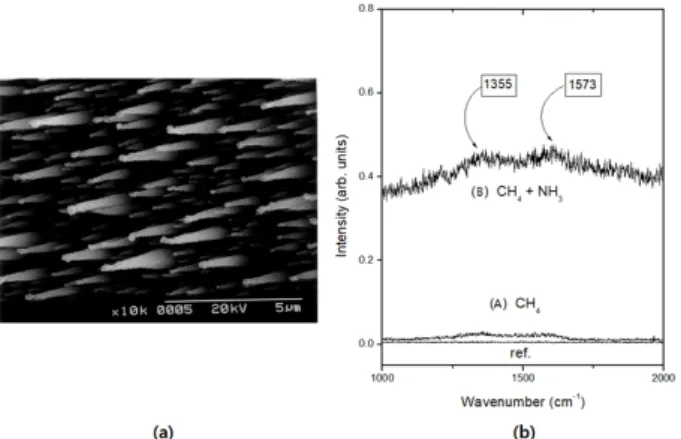
To use the carbon whisker as a field emission device, it must be driven at a low voltage to flow a large amount of current. Because the carbon whiskers are needle- shaped, they can exhibit improved field emission char- acteristics, compared to the case where diamonds are made in a pyramid shape using semiconductor process- ing. Therefore, in this study, we analyzed whether the field emission characteristics were improved by adding NH3, while growing the carbon whiskers. As shown in Fig. 5(a), when NH3was added, the shape of the carbon whisker changed into a sharp cone and the growth rate increased. This is because the nitrogen from NH3 de- composed, thereby inhibiting the formation and growth of the diamonds. This caused the carbon to remain in an amorphous state, which is precipitated as graphite by an applied bias voltage. It can be assumed that the cauliflowers are not visible on the surface of the thin film because a large amount of graphite was produced by adding the NH3. As shown in Fig. 5(b), (A) in the absence of NH3, there is almost no observable peak in the Raman spectrum. However, in the case of (B) NH3
addition, the peaks appear approximately at 1355 cm−1 and 1573 cm−1 in the Raman spectrum. Further, the small peak observed at 1355 cm−1 is a microcrystalline graphite peak. Furthermore, the main peak of graphite occurs at 1573 cm−1, which is slightly deviated from its expected position at 1580 cm−1. However, there is no peak corresponding to diamond. Therefore, from the Raman spectra, we can infer that the constituent of the carbon whisker is graphite.
4. Bias current dependent field emission charac- teristics of the carbon whiskers
The field emissions were measured using a setup as shown in inset of Fig. 6(b). Figure 6 shows the field emission graphs of a carbon whisker deposited by vary- ing the bias current. From Fig. 6(a), we can conclude that the emission current density increases proportion- ally with the bias current. This proportional increase can be attributed to the increased field emission area, which is obtained when the electrode is longer in the vertical direction.
Figure 6(b) shows the field emission graph of a carbon whisker deposited by applying a bias current of – 300
Fig. 5. (a) SEM image of the carbon whiskers. (b) Ra- man spectrum with NH3 = 100% in CH4under the fol- lowing conditions: Tf = 1920◦C, Ts= 850 ◦C, P = 20 torr, Vb = – 270 V, Ib = – 300 mA, and CH4 = 5%.
Fig. 6. (Color online) Field emission properties of the (a) carbon whiskers depending on the applied bias cur- rent and (b) nitrogen-doped carbon whiskers under the following conditions: Tf = 1920 ◦C, Ts = 950◦C, P = 20 torr, CH4 = 5%, Vb = – 270 V, Ib = – 300 mA), and NH3 = 100% in CH4.
mA and adding 100% (5 sccm) of NH3 to CH4. It can be seen that the operating voltage is significantly low- ered to 2 V/µm and the field emission current density is increased. As shown in Fig. 5(a), the field emission area increased as the carbon whisker grew longer in the verti- cal direction, and the operating voltage was significantly reduced, compared to the case of a nitrogen-doped dia- mond thin film. This implies that the work function of the thin film was lowered by nitrogen from the added NH3. Therefore, it can be concluded that increasing the bias current while adding NH3lowers the operating volt- age and increases the field emission current density.
longer, and the diameter of the whisker increased as the CH4 concentration and substrate temperature in- creased. This tendency is due to the increase in the bias current during the deposition. Further, the amount of emission current increases because of an increase in the electrode area in the vertical direction, and the highest charge density accumulates at the tip of the whiskers when the structure of a single whisker is in the form of a needle rather than a plane. Consequently, the number of emitted electrons increase. In addition, the current density of the nitrogen-doped carbon whiskers increased rapidly rather than the carbon whiskers deposited with- out nitrogen doping. In the case of the thin film to which a small amount of NH3 was added during the carbon whisker growth, the operating voltage was sig- nificantly reduced by 2 V/µm. This phenomenon occurs because the nitrogen from NH3decomposes, thereby de- creasing the formation and growth of diamond, and an applied bias voltage precipitates amorphous carbon into graphite. Therefore, the constituent of the whisker was graphite, and this fact was confirmed by Raman spectro- scopic analysis of the deposited thin film. As a result, the carbon whiskers can be driven, even in a weak electric field, as they exhibit characteristics of a good conductor.
Therefore, this study shows that a field emission device, consisting of carbon whiskers and having a low operat- ing voltage and high current density, can be grown on a silicon substrate by applying a bias current and with- out the aid of transition metals. An increase in the bias current and substrate temperature, and addition of NH3
during the deposition process are the key processes that facilitate the device fabrication.
ACKNOWLEDGEMENTS
This work is supported by Dong-A University.
REFERENCES
[1] C. A. Spindt, I. Brodie, L. Humphrey, and E. R.
Westerberg, J. Appl. Phys. 47, 5248 (1976).
[2] M. Z. Shamim, S. K. Persheyev, and M. J. Rose, in 2016 10th International Conference on Intelligent Systems and Control (ISCO), 1 (2016).
[3] X. Wang et al., Mater. Res. Express 5, 126403 (2018).
[4] M. Mertens and M. Mohr, J. of Nanomater. 26, 1 (2015).
[5] D. Eremchenko, V. I. Makhov, E. I. Shulgin, and V. A. Fedirko, Diffusion tip shaping under vacuum breakdown, in IVMC ’95. Eighth International Vac- uum Microelectronics Conference. Technical Digest (Cat. No.TH8012), Portland, OR, USA, 1995, pp.
92.
[6] Q. H. Wang et al., Appl. Phys. Lett. 72, 2912 (1998).
[7] W. Kulish et al., Diam. Relat. Mater. 6, 906 (1997).
[8] A. K. Both and C. L. Cheung, RSC Adv. 9, 23780 (2019).
[9] S. Lukashenko et al., J. Phys: Conf. Series 769, 012062 (2016).
[10] J. Liu et al., J. Vac. Sci. Technol. B 13(2), 422 (1995).
[11] V. V. Zhirnov, A. B. Voronin, E. I. Givargizov, and A. L. Meshcheryakova, J. Vac. Sci. Technol.
B 14(3), 2034 (1996).
[12] V. V. Zhirnov et al., J. Vac. Sci. Technol. B 15(2), 446 (1997).
[13] K. C. Park, J. H. Moon, S. J. Chung, and J. Jang, J. Vac. Sci. Technol. B 15(2), 454 (1997).
[14] M. Park et al., J. Vac. Sci. Technol. B 17(2), 734 (1999).
[15] T. Sato et al., Appl. Phys. Lett. 66(2), 159 (1995).
[16] K. Haraguchi et al., Appl. Phys. Lett. 69(3), 386 (1996).
[17] Z. F. Ren et al., Science 282, 1105 (1998).
[18] W. Zhu et al., Appl. Phys. Lett. 75(6), 873 (1999).
[19] J. Kennedy et al., Diam. Relat. Mater. 71, 79 (2017).
[20] S. Helveg, J. Sehested, and J.R. Rostrup-Nielsen, Catal. Today 178, 42 (2011).
[21] S. H. Tsai, C. W. Chao, C. L. Lee, and H. C. Shih, Appl. Phys. Lett. 74(23), 3462 (1999).