DOI:10.5369/JSST. 2011.20.3.156 pISSN 1225-5475/eISSN 2093-7563
UV Responsive Characteristics of n-Channel Schottky Barrier MOSFET with ITO as Source/Drain Contacts
Tae-Hyeon Kim1, Chang-Ju Lee1, Dong-Seok Kim1, Sang-Yun Sung2, Young-Woo Heo2, Jung-Hee Lee1, and Sung-Ho Hahm1,+
Abstract
We fabricated a schottky barrier metal oxide semiconductor field effect transistor(SB-MOSFET) by applying indium-tin-oxide(ITO) to the source/drain on a highly resistive GaN layer grown on a silicon substrate. The MOSFET, with 10 μm gate length and 100 μm gate width, exhibits a threshold gate voltage of 2.7 V, and has a sub-threshold slope of 240 mV/dec taken from the IDS-VGScharacteristics at a low drain voltage of 0.05 V. The maximum drain current is 18 mA/mm and the maximum transconductance is 6 mS/mm at VDS=3 V. We observed that the spectral photo-response characterization exhibits that the cutoff wavelength was 365 nm, and the UV/visible rejection ratio was about 130 at VDS= 5 V. The MOSFET-type UV detector using ITO, has a high UV photo-responsivity and so is highly applicable to the UV image sensors.
Keywords : Highly resistive GaN, Schottky Barrier MOSFET, ITO, UV responsivity
1. INTRODUCTION
Gallium nitride(GaN) is one of the most promising materials for both opto-electronic devices, such as high sensitive ultraviolet(UV) detector, visible light emission diode(LED) and high temperature / high frequency / high power electronic devices, such as high electron mobility transistor(HEMT)[1-3], metal insulator semiconductor field effect transistor(MISFET)[4, 5].
At least until recently, there has not been much interest in enhancement mode transistors, even though there are many applications for integrated UV image sensors as well as high power logic integrated circuit applications.
Schottky barrier source/drain(S/D) structure MISFET and silicon implanted S/D MISFET have been presented in [6]
and [7], respectively. The schottky barrier S/D is an attractive solution because it excludes the use of the high cost S/D ion implantation process and very high temperature activation at over 1500 。C[1]. Indium-tin- oxide(ITO), on the other hand, has been widely applied to many other opto-electronic devices because of its highly
conductive and visible-transparent properties[8].
In this study, we investigated both the electrical and the UV responsive characteristics of a fabricated enhancement mode n-channel SB-MOSFET using ITO schottky barrier S/D on a highly resistive GaN layer grown on a silicon substrate in the near UV and visible regions for the various gate/drain bias conditions. The fabricated devices exhibit very promising behaviors, such as a very high on/off current ratio, high transconductance, and a good UV/visible rejection ratio.
2. THE DEVICE FABRICATION
Fig. 1 shows a schematic of the cross-sectional view of the epitaxial GaN layer structure. The epitaxial GaN layer for the MOSFET was grown on an n-type Si(111) substrate using metal-organic chemical vapor deposition(MOCVD) by using TMGa, TMAl, and NH3as the precursors for Ga, Al, and N, respectively. First, a Si(111) substrate was cleaned by diluted HF in other to remove the native oxides, and then a 150 nm-thick high-temperature(HT) AlN buffer was grown at 1100 。C in other to prevent an occurrence of the meltback etching attributed to the Ga-Si reaction. To release the strong tensile stress between the GaN and the Si substrate caused by the large differences in the lattice constant and thermal expansion coefficient, a 170 nm-thick
1School of Electrical Engineering and Computer Science, Kyungpook National Unversity
2School of Materials Science and Engineering, Kyungpook National Unversity
+Corresponding author: [email protected]
(Received : Jan. 19, 2011, Revised : May. 13, 2011, Accepted : May 6, 2011)
high temperature(HT) GaN and a 30 nm-thick low- temperature(LT) AlN interlayers were periodically grown by five times. The LT-AlN interlayer, especially, plays a main role in the tensile stress reduction[9, 10]. Finally, a 0.7 um-thick crack-free and highly resistive GaN layer was grown at 1070 。C. The growth pressure of proposed structure was fixed at 100 torr.
In order to measure the transmittance of the ITO contact electrode, we first deposited ITO onto glass substrates by an RF sputtering system from a target composed of 90 % In2O3and 10 % SnO2. During the ITO deposition, we kept the deposition condition at 10 mTorr in Ar/O2 atmosphere(Ar : O2= 1000 : 1). The thickness of the ITO layers was kept at 1000 Å throughout this study. In some cases, the as-deposited ITO films were thermally annealed in air atmosphere from 300 。C to 700 。C for 15 min. The transmission spectra of the as-deposited ITO, the thermally annealed ITO were measured using a VARIAN UV-VIS- NIR spectrometer.
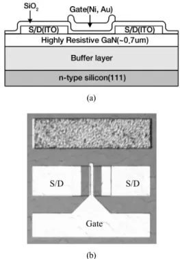
Fig. 2 shows a schematic of the cross-sectional diagram and the top-view image of the fabricated SB-MOSFET.
Before the deposit of the gate dielectric and the S/D ITO’s, the wafers were dipped in a diluted hydrochloric acid water solution(HCl : H2O = 1 : 1) for 3 min to remove the native
oxides. We then deposited a 1000 Å ITO layer at room temperature onto the GaN epitaxial layers to apply for the schottky barrier source and drain. SiO2(320 Å) deposition was followed for the gate dielectric using the PECVD method at 300 。C. Finally, Ni(400 Å)/Au(500 Å) was deposited as the gate metal and bonding pads of S/D by e- beam evaporator. An Agilent 4156C semiconductor parameter analyzer was used to measure the current- voltage(I-V) characteristics of the fabricated SB-MOSFET.
A xenon arc lamp was used as the optical source for the spectral responsivity measurements. A calibrated UV- enhanced Si detector was used for signal detection.
3. THE RESULTS AND DISCUSSIONS
Fig. 1. (a) The schematic cross section and (b) the growth temperature as a function of growth time of the epitaxial layer structure grown on silicon, which incorporates multiple HT- GaN and LT-AlN interlayers.
(b) (a)
Fig. 2. (a) The schematic cross section and (b) the top-view image of the fabricated SB-MOSFET.
(b) (a)
Fig. 3. The optical transmittance characteristic variations regarding the annealing temperature for 1000 Å-thick ITO films under air atmosphere for 15 min.
Fig. 3 shows the transmission spectra of the as-deposited ITO and thermally annealed ITO layers. In this figure, the transmittance of each film was normalized with respect to the transmittance of the glass substrate. It can be seen that the as-deposited ITO has a peak 80 % transmittance at 400 nm. However, after a 15 min thermal annealing at 300 。C in air atmosphere, we observed a significant improvement in its optical properties. We found that ITO became more transparent in all of the wavelengths of interest. We also found that the peak transmittance increased from 80 % to 86 %. The peak wavelength was also blue-shifted from 400 to 375 nm. Table 1 shows the ITO electrical properties evolution with the annealing temperature in air. We can confirm that the as-deposited ITO film has 5.0×10⁻⁴Ω· cm at room temperature(25 。C). The ITO film properties are not strongly affected by the annealing temperature at 300 。C, as can be seen by analyzing the ρand n values.
The obtained results are not presented here due to space limitations, but the air annealing over 300 。C leads to films with deteriorated properties. For instance, the ρof the ITO films increases from ~ 5.0×10⁻⁴Ω·cm at R.T. to ~ 7.4×
10-3Ω·cm at 700 。C and the mobility(μ) decreases from ~ 22.8 cm2/V·s at R.T. to ~ 0.2 cm2/V·s at 700 。C.
The fabricated GaN SB-MOSFET with 10 μm gate length and 100 μm gate width on the silicon exhibited normally-off operation with threshold voltage of 2.7 V, by extrapolation of the transfer I-V characteristics in the linear region at VDS= 0.05 V. Observing the photoluminescence (PL) spectrum of the highly resistive GaN epitaxial layer grown on the silicon, as shown in Fig. 4, it exhibits a band edge peak at a wavelength of 360 nm. This is a meaningful result for the possibility of GaN MOSFET and its applications to high power logic, switching, and opto- electronic devices.
The output I-V characteristics of the fabricated SB-
Fig. 4. The photoluminescence spectrum of the epitaxial GaN layer grown on silicon used in this work.
Fig. 5. The IDS-VDScharacteristic of the SB-MOSFET using ITO source /drain.
Fig. 6. The IDS-VGScharacteristics of the SB-MOSFET using ITO S/D at VDS= 0.05 V.
Fig. 7. The IDS-VGSand transconductance of the SB-MOSFET using ITO S/D at VDS= 3 V.
n [ cm-3 ] μ[ cm2/V·s ] σ[ 1/Ω·cm ] ρ[ Ω·cm ]
as-deposited 5.461E+20
2.281E+1 1.995E+3 5.011E-4
300 。C annealed 7.639E+20
1.220E+1 1.493E+3 6.696E-4 Table 1. The electrical properties of the ITO films on glass.
MOSFET with ITO S/D is shown in Fig. 5 which exhibits better characteristics compared to those of the SB- MOSFET with Al S/D fabricated similarly[4]. The workfunction of ITO is 4.3 eV that is almost equivalent to the electron affinity of GaN, there is only a slight conduction band energy barrier caused by the interface states between ITO S/D and GaN. The fabricated device with ITO S/D has 18 mA/mm of the maximum drain current and 6 mS/mm of the maximum transconductance at VDS= 3 V. Fig. 6 shows the typical linear and logarithmic ID-VGScharacteristics of the fabricated SB-MOSFET. The fabricated device has 240 mV/dec of a sub-threshold slope and 109of on/off ratio at VDS= 0.05 V. The superior on/off ratio can be attributed to the high schottky hole barrier at the source and drain contacts.
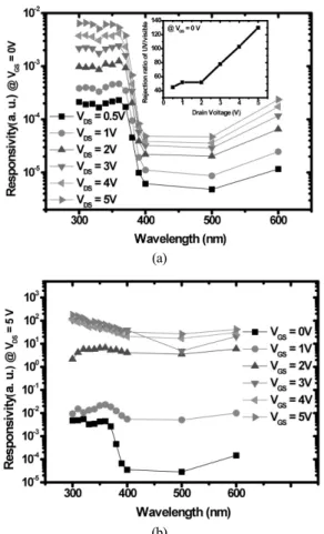
Fig. 8(a) shows the variations in the spectral responsivity of IDaccording to the drain biases VDSat VGS= 0 V, which is the same condition as that of the MSM-type photodetector. This shows that the UV/visible rejection ratio increases by augmenting the drain voltage. The cutoff
wavelength was about 365 nm, and the highest UV/visible rejection ratio of 130 was observed at VDS= 5 V. The high photocurrent and high UV/visible rejection ratio might be attributed to the high transparency of the 300 。C annealed ITO S/D electrodes, since the transparent ITO electrodes could increase the effective active areas and thereby increase the number of photo-generated carriers. The slowly increasing responsivity in accordance to the bias, which is above the cutoff wavelength, is due to the surface leakage current through the incompletely passivated GaN surface under the PECVD gate oxide layer. In addition, the traps, related to the yellow peaks seen in Fig. 4, may degrade the UV sensitivity and selectivity. If the higher quality SiO2is applied and we can optimize the GaN layer quality, the UV responsivity and selectivity will be much improved. Fig. 8(b) shows the spectral response of drain current according to the gate biases VGSat a constant VDS
of 5 V. No spectral dependence of the gate voltage has been observed. The ratio decreased rapidly down to 0 at VGS> 1 V, where the inversion electrons become the major player of the channel current. Therefore, if we tightly control between VGS= 0 V and 1 V, the GaN layer would be depleted and UV/visible rejection ratio could be increased as the drain voltage increases.
4. CONCLUSION
We demonstrated the schottky barrier metal oxide semiconductor field effect transistor applying ITO transparent electrodes as the source and drain on the highly resistive GaN layer grown on the silicon substrate. The ITO S/D MOSFET exhibited excellent characteristics, such as the maximum current of 18 mA/mm and the maximum transconductance of 6 mS/mm at VDS= 3 V. We also investigated the UV responsive characteristics of SB- MOSFET. Through the spectral UV response characterization, the cutoff wavelength was 365 nm, and the UV/visible rejection ratio was about 130 at VDS= 5 V and VGS= 0 V. Therefore, ITO is a promising material for the source and drain of GaN SB-MOSFETs. If we optimize the GaN layer quality, the UV responsivity and selectivity will be greatly improved. In addition, it is easy to integrate this type of photodetector with an enhancement type MOSFET logic circuit on the GaN layer.
Fig. 8 (a) The spectral responsivity variations according to drain biases at VGS= 0 V and (b) the spectral responsivity variations according to gate biases at VDS= 5 V.
(b) (a)
ACKNOWLEDGMENT
This work was partially supported by Brain Korea 21(BK21), the National Research Foundation of Korea(NRF) grant funded by the Korea govern- ment(MEST)(No. 2011-0001068), and the World Class University(WCU) program through the Korea science and Engineering Foundation funded by the Ministry of Education, Science and Technology(R33-10055)
REFERENCES
[1] H. Yu, L. McCarthy, S. Rajan, S. Keller, S. Denbaars, J. Speck, and U. Mishra, “Ion implanted AlGaN-GaN HEMTs with nonalloyed ohmic contacts,” IEEE Electron Device Lett., vol. 26, no. 5, pp. 283-285, 2005.
[2] K. Shiojima, T. Sugahara, and S. Sakai, “Large schottky barrier for Ni/p-GaN contacts,” Appl. Phys.
Lett., vol. 74, no. 14, pp. 1936-1938, 1999.
[3] J. I. Pankove, “Perspective on gallium nitride,” in Proc.
Master. Res. Soc., vol.162, pp. 515-519, 1990.
[4] H.-B. Lee, H.-I. Cho, H.-S. An, J.-H. Lee, and S.-H.
Hahm, “Enhancement mode operation and ultraviolet responsivity of n-channel GaN metal-insulator- semiconductor field effect transistor with schottky barrier source and drain,” Jpn. J. Appl. Phys., vol. 46, no. 4B, pp. 2348-2351, 2007.
[5] H.-B. Lee, H.-I. Cho, H.-S. An, Y.-H. Bae, M.-B. Lee, J.-H. Lee, and S.-H. Hahm, “A normally off GaN n- MOSFET with schottky-barrier source and drain on a Si-auto-doped p-GaN/Si,” IEEE Electron Device Lett., vol. 27, no. 2, pp. 81-83, 2006.
[6] W. Huang, T. Khan, and T. P. Chew, “Enhancement- mode n-channel GaN MOSFETs on p and n- GaN/Sapphire substrate,” IEEE Electron Device Lett., vol. 27, no. 10, pp. 796-798, 2006.
[7] H. Kambayashi, Y. Niiyama, S. Ootomo, T. Nomura, M. Iwami, Y. Satoh, S. Kato, and S. Yoshida,
“Normally off n-channel GaN MOSFETs on Si substrates using an SAG technique and ion implantation,” IEEE Electron Device Lett., vol. 28, no.
12, pp. 1077-1079, 2007.
[8] T. Margalith, O. Buchinsky, D. A. Cohen, A. C. Abare, M. Hansen, S. P. DenBaars, and L. A. Coldren,
“Induim tin oxide contacts to gallium nitride optoelectronic devices,” Appl. Phys. Lett., vol. 74, no.
26, pp. 1930-1932, 1999.
[9] A. Dadgar, J. Blasing, A. Diez, A. Alam, M. Heuken, and A. Krost, “Metalorganic chemical vapor phase epitaxy of crack-free GaN on Si(111) exceeding 1 um in thickness”, Jpn, J. Appl. Phys., vol. 39, no. 11B, pp.
L1183-L1185, 2000.
[10] A. Krost and A. Dadgar, “GaN-based devices on Si”, Phys. Stat. Sol. (a), vol.194, no. 2, pp. 361-375, 2002.
Tae-Hyeon Kim received the M.S.
degree from the School of Electrical Engineering and Computer Science at Kyungpook National University, Daegu, Korea. His current research is focused on the study of gallium nitride- based MOSFETs and ultraviolet(UV) image sensors.
Chang-Ju Lee received the B.S. degree in Electrical Engineering and Computer Science from Kyungpook National University, Korea. He is currently working toward the M.S degree in Prof.
Hahm's group at Kyungpook National University. His current research is focused on the study of UV image sensors and GaN schottky barrier MOSFETs.
Dong-Seok Kim received the M.S.
degree from the School of Electrical Engineering and Computer Science at Kyungpook National University, Daegu, Korea in 2010, and is working toward the Ph.D. degree. His current research is focused on the growth of gallium-nitride-based materials and the fabrication of normally-off GaN devices.
Sang-Yun Sung received the B.S. and M.S. degree from the School of Materials Science and Engineering at Kyungpook National University, Daegu, Korea. He is now conducting research in pursuit of the Ph.D degree under Prof. Young-Woo Heo at Kyungpook National University. His current research is focused on thin films, nanowires, and transparent oxide semiconductor devices for their application in displays, solar cells, sensors, and transparent electronics.
Young-Woo Heo received the Ph.D.
degree in Materials Science and Engineering, from the University of Florida in 2003. He is a professor in the School of Materials Science and Engineering, College of Engineering at Kyungpook National University. His current research interests include thin films, nanowires, and transparent oxide semiconductor devices for their application in displays, solar cells, sensors, and transparent electronics.
Jung-Hee Lee received the Ph.D.
degree in Electrical and Computer Engineering from North Carolina State University, Raleigh, in 1990. He has been a Professor at the School of Electronics Engineering, College of IT Engineering at Kyungpook National University since 1993. His current research is focused on the growth of nitride-based materials and the fabrication and characterization of gallium-nitride-based electronics and optoelectronic devices.
Sung-Ho Hahm received the M.S. and Ph.D. degrees in Electronic Engineering from the Korea Advanced Institute of Science and Technology(KAIST) in 1987, and 1991, respectively. During 2003, he was a chief at the National Education Center for Semiconductor Technology(NECST). He is a professor at the School of Electrical Engineering, College of IT Engineering at Kyungpook National University. His current research interests include GaN based UV opto-electronic devices, and 3-dimensional field effect transistors.