http://dx.doi.org/10.5369/JSST.2018.27.6.362 pISSN 1225-5475/eISSN 2093-7563
CMOS Binary Image Sensor with Gate/Body-Tied PMOSFET-Type Photodetector for Low-Power and Low-Noise Operation
Junwoo Lee, Byoung-Soo Choi, Donghyun Seong, Jewon Lee, Sang-Hwan Kim, Jimin Lee, Jang-Kyoo Shin, and Pyung Choi
+Abstract
A complementary metal oxide semiconductor (CMOS) binary image sensor is proposed for low-power and low-noise operation.
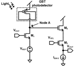
The proposed binary image sensor has the advantages of reduced power consumption and fixed pattern noise (FPN). A gate/body- tied (GBT) p-channel metal-oxide-semiconductor field-effect transistor (PMOSFET)-type photodetector is used as the proposed CMOS binary image sensor. The GBT PMOSFET-type photodetector has a floating gate that amplifies the photocurrent generated by incident light. Therefore, the sensitivity of the GBT PMOSFET-type photodetector is higher than that of other photodetectors.
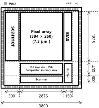
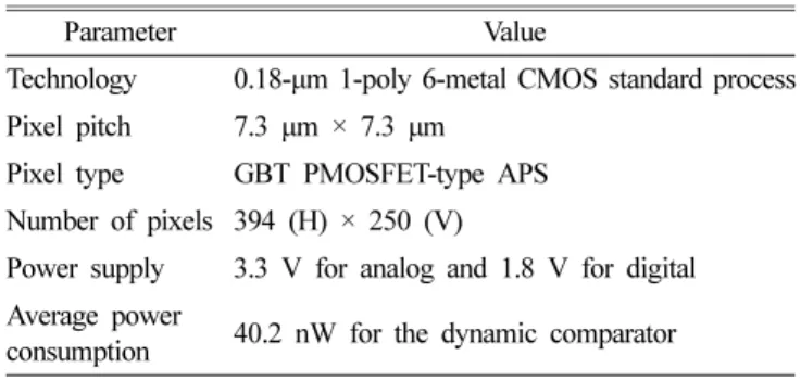
The proposed CMOS binary image sensor consists of a pixel array with 394 (H) × 250 (V) pixels, scanners, bias circuits, and col- umn parallel readout circuits for binary image processing. The proposed CMOS binary image sensor was analyzed by simulation.
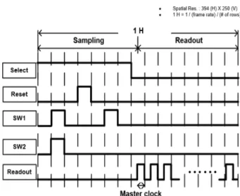
Using the dynamic comparator, a power consumption reduction of approximately 99.7% was achieved, and this performance was verified by the simulation by comparing the results with those of a two-stage comparator. Also, it was confirmed using simulation that the FPN of the proposed CMOS binary image sensor was successfully reduced by use of the double sampling process.
Keywords: CMOS image sensor, Binary image sensor, GBT PMOSFET-type photodetector, Dynamic comparator
1. INTRODUCTION
Recently, the demand for CMOS image sensors has increased with the proliferation of smartphones and wearable devices.
Compared with the charge-coupled device (CCD) image sensor, the CMOS image sensor, fabricated using a standard CMOS process, has several advantages such as high integration, low power, and low cost [1-3]. There are several considerations in designing a CMOS image sensor, such as low power, high-speed operation, wide dynamic range, and high sensitivity [4-6]. Among these, low power and low-noise operation are the most important considerations for portable devices.
The types of photodetector for image sensors are the GBT PMOSFET-type photodetector, avalanche photodiode (APD), bipolar junction transistor (BJT) photodetector, and p-n junction
photodiode. The APD requires a high voltage for breakdown, and the BJT photodetector occupies a large area in an active pixel sensor (APS). In addition, the p-n junction photodiode has low sensitivity. However, the proposed GBT PMOSFET-type photodetector has several advantages such as low power, small area, and high sensitivity compared with other photodetectors [7].
The CMOS binary image sensor has good noise characteristics such as reset noise, thermal noise, and FPN because it has one-bit digital output [8]. In addition, if binary image processing is used, additional analog-to-digital conversion is not required. Therefore, the binary image sensor has advantages in terms of low noise and low power. The CMOS binary image sensor has a short exposure time if it operates at high speed. Therefore, a high-sensitivity photodetector is necessary to compensate the signal voltage for the CMOS binary image sensor.
In previous research, a CMOS binary image sensor with a GBT PMOSFET-type photodetector was proposed [9]. The present paper proposes a CMOS binary image sensor with a GBT PMOSFET-type photodetector for low-power and low-noise operation. Dynamic comparators are used instead of usual two- stage comparators in the readout circuits to realize low power consumption. The FPN is reduced by using a double sampling circuit, which is composed of capacitors and CMOS switches. The capacitors and resistors in the readout circuits were optimized by School of Electrical Engineering, Kyungpook National Unversity
Sangyeok 3-dong, Buk-gu, Daegu, 41566, Korea.
+