• 검색 결과가 없습니다.

High-Speed CMOS Binary Image Sensor with Gate/Body-Tied PMOSFET-Type Photodetector

N/A
N/A
Protected

Academic year: 2021

Share "High-Speed CMOS Binary Image Sensor with Gate/Body-Tied PMOSFET-Type Photodetector"

Copied!
5
0
0

로드 중.... (전체 텍스트 보기)

전체 글

(1)

In this paper, we propose a complementary metal oxide semiconductor (CMOS) binary image sensor with a gate/body-tied (GBT) PMOSFET-type photodetector for high-speed operation. The GBT photodetector of an active pixel sensor (APS) consists of a floating gate (n

+

-polysilicon) tied to the body (n-well) of the PMOSFET. The p-n junction photodiode that is used in a conventional APS has a good dynamic range but low photosensitivity. On the other hand, a high-gain GBT photodetector has a high level of photosensitivity but a narrow dynamic range. In addition, the pixel size of the GBT photodetector APS is less than that of the conventional photodiode APS because of its use of a PMOSFET-type photodetector, enabling increased image resolution. A CMOS binary image sensor can be designed with simple circuits, as a complex analog to digital converter (ADC) is not required for binary processing. Because of this feature, the binary image sensor has low power consumption and high speed, with the ability to switch back and forth between a binary mode and an analog mode. The proposed CMOS binary image sensor was simulated and designed using a standard CMOS 0.18 µm process.

Keywords: CMOS image sensor, Binary image, High speed, Gate/body-tied photodetector

1. INTRODUCTION

Currently, CMOS devices and charge-coupled devices (CCDs) are used for image sensors. Although CMOS image sensors (CISs) have fixed pattern noise (FPN), their advantages in terms of low cost, high speed, and high integration have led to their replacement of CCD image sensors in many applications, including mobile phones, digital cameras, security devices, and medical and automotive devices. In CISs, power efficiency is essential because the battery power of portable devices is limited.

High-speed operation of the image sensor also becomes important as the resolution increases [1-8].

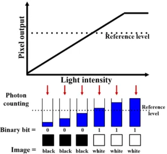
The CIS can be designed as a binary image processing unit using the standard CMOS technology. A conventional CIS has complex circuits, such as an amplifier, an analog-to-digital converter (ADC), and a noise canceller, to ensure high contrast and multiple bit

information. These complex operations can easily be simplified using the readout circuits in a binary image sensor. The binary process can be implemented using a simple comparator and memory and can have very high speed. The binary image sensor is interesting because the captured image in a binary form can be processed using fast logical operations [9,10]. Such a sensor is used in various applications, including bar-coding, fingerprint and character recognition, motion detectors, and edge detectors.

The photodetectors used in the image sensors are conventionally bipolar junction transistor (BJT) photodetectors, silicon-on-insulator (SOI) photodetectors, hole accumulation diodes (HADs), and pinned photodiodes [11-14]. We propose a CMOS binary image sensor using a GBT PMOSFET-type photodetector. The high-gain GBT photodetector has a high level of photosensitivity [15,16]. The GBT photodetector does not require the use of a special fabrication process; it can be designed using a standard CMOS process. The proposed CMOS binary image sensor using a GBT photodetector was simulated and designed using a standard CMOS 0.18 ìm process.

2. OPERATION PRINCIPLE

2.1 Active Pixel Sensor

Fig. 1(a) shows a schematic diagram of a conventional

1

School of Electronics Engineering,

2

Department of Sensor and Display Engineering,

Kyungpook National University, 80 Deahakro, Buk-gu, Daegu 702-701, Korea

+

Corresponding author: [email protected] (Received : Aug. 29, 2014, Accepted : Sep. 18, 2012)

This is an Open Access article distributed under the terms of the Creative Commons Attribution Non-Commercial License(http://creativecommons.org/

licenses/bync/3.0) which permits unrestricted non-commercial use, distribution,

and reproduction in any medium, provided the original work is properly cited.

(2)

photodiode active pixel sensor (APS). It is composed of 3 transistors (M1–3) and a p-n junction photodiode. M1 resets the floating diffusion (FD) node, M2 serves as a source follower for amplifying the pixel signal, and M3 performs row selection. M4 is a transistor for biasing the source follower and is located outside of the pixel. Electron-hole pairs (EHPs) are generated in the depletion layer of the photodiode. The conventional photodiode APS has low sensitivity because of the large capacitance of the FD node. Fig. 1(b) shows a schematic diagram of the proposed APS. The proposed pixel is made up of the GBT photodetector and 3 transistors. The body of the GBT PMOSFET-type photodetector is tied to the gate. The light is incident through the gate. The operation of the 3 transistors (M1–3) and the bias transistor (M4) is the same as in the conventional photodiode APS. The GBT photodetector has high responsivity and is used for a high-speed CMOS binary image sensor. The output signal of

the GBT APS has a linear response to the light intensity.

A cross-sectional view of the GBT photodetector is shown in Fig. 2. The floating gate of the GBT photodetector is tied to the n-well body, similar to that of the conventional PMOSFET. The source of the GBT photodetector is connected to the V

DD

, and the drain is connected to the floating diffusion (FD) node. In the case of the GBT photodetector, the light is incident on the gate (polysilicon) and the body (n-well). The EHPs generated by the incident light affect the gate/body potential. The GBT photodetector signals are later amplified.

Fig. 3 shows the layout of the proposed APS. The pixel size of the APS is 5.6 µm×5.6 µm. The pixel size design takes into consideration the column parallel binary processing and the optics of the pixel. A metal shield layer is used to block light. The light that contributes to the APS output signal is incident on the part not covered with the shield metal. The open region of the metal has a size of 1 µm × 0.6 µm and is much smaller than that in a typical photodiode. It is possible to design the chip with the pixel size Fig. 1. Schematic diagram of (a) the conventional photodiode APS

and (b) the proposed APS.

Fig. 2. Cross-sectional view of the GBT photodetector.

Fig. 3. Layout of the proposed APS.

(3)

reduced even further. The proposed GBT photodetector was designed using a standard CMOS 0.18 µm process.

2.2 Binary Processing

Fig. 4 shows a schematic diagram of the APS with the binary processing circuit. The output signal of the pixel is fed as input to the comparator and compared with a reference voltage. The reference voltage determines the function of the binary processing. The image after binary processing is represented to only black and white, with the number of black increasing with the reference voltage, and the number of white increasing with a decrease in the reference voltage. It is therefore important to set the reference voltage accurately to obtained the desired correct output voltage from the pixel.

A diagram illustrating the binary processing is shown in Fig. 5.

The output signal increases linearly in response to the illuminating light, owing to the charge generated by the increasing number of photons at the FD node. When it exceeds the reference level while counting photons, the binary output bit changes to 1 and the image is represented by white pixels. Binary processing does not require an ADC, and the binary image sensor can be operated at high speeds by taking advantage of the high responsivity of the GBT APS.

Fig. 6 shows a schematic diagram of the proposed CMOS binary image sensor, composed of the pixel array, column parallel binary processing circuits, multiplexer (MUX), and

binary output buffer. The column parallel binary processing circuits consist of a comparator, memory, and digital buffer. The binary processing circuits are simple and occupy a small area on the chip but play a powerful role in the high-speed operation of the image sensor.

Fig. 4. Schematic diagram of APS with binary processing circuit.

Fig. 5. Diagram illustrating the principle of the binary processing.

Fig. 6. Schematic diagram of CMOS binary image sensor.

(4)

3. SIMULATION AND DISCUSSIONS

3.1 Simulation

We simulated a computational circuit using Cadence Spectre with a simulation library of a standard 0.18 µm CMOS process.

Fig. 7 shows the simulation results of the output voltage for the photodetector type of APS. The simulation of the APS was based on an exposure time of 10 ms. The output voltage of the

photodiode APS varies from 2.3 to 0 V by changing the photocurrent, and the output voltage of the GBT APS varies from 0.93 to 2.2 V. Although the GBT APS has the disadvantage of a narrow output swing, the response of the GBT APS is faster than that of the photodiode APS, indicating that the GBT APS has high responsivity even under low illumination.

The timing diagram of the CMOS binary image sensor using the GBT APS is shown in Fig. 8. As the photocurrent increases, the slope of the graph increases and the output signal of the GBT APS is saturated at an early stage. It is possible to change the reference voltage. When the output signal of the GBT APS is less (greater) than the reference voltage, the output of the comparator is low (high). The output signal of the comparator becomes therefore the binary bit of the binary image sensor.

3.2 Discussion

In comparison with the conventional CMOS image sensor, the proposed binary image sensor has low power consumption and high speed and with a simpler circuit too, because an ADC is not required. It is also possible to reduce the pixel size, enabling a large number of pixels to be fabricated on the chip. Fig. 9 shows the layout of the proposed CMOS binary image sensor, composed of a GBT pixel array (176 × 144), binary processing circuits, MUXes, and a scanner. The size of the entire image sensor is small at 1.3 mm × 1.5 mm. The image sensor that we present can be switched between a binary mode and an analog mode. The Fig. 7. Variation in the output voltage with the photocurrent as a type

of photodetector (simulation results).

Fig. 8. Timing diagram of CMOS binary image sensor using GBT APS (simulation results).

Fig. 9. Layout of the proposed CMOS binary image sensor.

(5)

simple circuit with low power consumption, high resolution, and high-speed operation. We expect the image sensor to operate at a high speed of more than 200 frames per second. The proposed image sensor with a high speed operation can be applied to various applications. In addition, it is possible to switch the sensor between the binary mode and the analog mode or vice versa.

ACKNOWLEDGMENT

This work was supported by the National Research Foundation of Korea (NRF) grant funded by the Korea government (MSIP) (No. 2008-0062617), the Center for Integrated Smart Sensors funded by the Ministry of Education, Science and Technology as Global Frontier Project (CISS-2011-0031868), the BK21 Plus program and the Integrated Circuit Design Education Center (IDEC) in Korea.

REFERENCES

[1] M. Bigas, E. Cabruja, J. Forest, and J. Salvi, “Review of CMOS image sensors”, Microelectronics J., Vol. 37, No. 2, pp. 433-451, 2006.

[2] R. H. Nixon, S. E. Kemeny, B. Pain, C.O. Staller, and E.R.

Fossum, “256 × 256 CMOS active pixel sensor camera-on- a-chip”, IEEE J. Solid-State Circuits, Vol. 31, No. 12, pp.

2046-2050, 1996.

[3] N. Stevanovic, M. Hillegrand, B. J. Hostica and A. Teuner,

“A CMOS image sensor for high-speed imaging”, IEEE International Solid-State Circuits Conference, pp. 104-105, 2000.

[4] S. Mendis, Sabrina E. Kemeny, and Eric R. Fossum,

“CMOS active pixel image sensor”, IEEE Trans. Electron Devices, Vol. 41, No. 3, pp. 452-453, 1994.

[5] M. Furuta, Y. Nishikawa, T. Inoue, and S. Kawahito, “A

[8] N. Kawai and S. Kawahito, “Noise analysis of high-gain, low-noise column readout circuits for CMOS image sen- sors”, IEEE Trans. Electron Devices, Vol. 51, No. 2, pp.

185-194, 2004.

[9] C. S. Hong and R. Hornsey, “On-chip binary image pro- cessing with CMOS image sensor”, Proc. SPIE, Vol. 4669, pp. 125-136, 2002.

[10] B. Zhang, K. Mei, and N. Zheng, “Reconfigurable pro- cessor for binary image processing”, IEEE Trans. Biomed.

Circuits Syst., Vol. 5, pp. 64-82, 2013.

[11] N. Tanaka, T. Ohmi, and Y. Nakamura, “A novel bipolar imaging device with self noise reduction capability”, IEEE Trans. Electron Devices, Vo. 36, pp. 31-38, 1989.

[12] K. Yonemoto and H. Sumi, “A CMOS image sensor with a simple fixed-pattern-noise-reduction technology and a hole accumulation diode,” IEEE J. Solid-State Circuits, Vol. 35, No. 12, pp.2038-2043, 2000.

[13] R. M. Guidash, T. H. Lee, P. P. K. Lee, D. H. Sackett, C. I.

Drowley, M. S. Swenson, L. Arbaugh, R. Hollstein, F. Sha- piro, and S. Domer, “A 0.6 ìm CMOS pinned photodiode color imager technology”, IEDM Technical Digest, pp. 927- 929, 1997.

[14] I. Brouk, K. Alameh, and Y. Nemirovsky, “Design and characterization of CMOS/SOI image sensors”, IEEE Trans. Electron Devices, Vol. 54, No. 3, pp. 468-475, 2007.

[15] S. H. Seo, S. H. Lee, M. Y. Do, J. K. Shin, and P. Choi,

“Highly and variably sensitive complementary metal oxide semiconductor active pixel sensor using P-channel metal oxide semiconductor field effect transistor-type photode- tector with transfer gate”, Jpn. J. Appl. Phys., Vol. 45, No.

4B, pp. 3470-3474, 2006.

[16] S. H. Seo, K. D. Kim, M. W. Seo, J. S. Kong, J. K. Shin, and P. Choi, “Optical characteristics of an n-well/gate-tied PMOSFET-type photodetector with built-in transfer gate for CMOS image sensor”, Sens. Mater., Vol. 19, No. 7, pp. 435- 444, 2007.

[17] M. Bae, S. H. Jo, M. Lee, J. Y. Kim, J. Choi, P. Choi, and

J. K. Shin, “A wide dynamic range CMOS image sensor

based on a pseudo 3-transistor active pixel sensor using

feedback structure”, J. Sensor Sci. & Tech., Vol. 21, No. 6,

pp. 413-419, 2012.

수치

Fig. 2. Cross-sectional view of the GBT photodetector.
Fig. 4 shows a schematic diagram of the APS with the binary processing circuit. The output signal of the pixel is fed as input to the comparator and compared with a reference voltage
Fig. 7 shows the simulation results of the output voltage for the photodetector type of APS

참조

관련 문서