• 검색 결과가 없습니다.

Simulation of High-Speed and Low-Power CMOS Binary Image Sensor Based on Gate/Body-Tied PMOSFET-Type Photodetector Using Double-Tail Comparator

N/A
N/A
Protected

Academic year: 2021

Share "Simulation of High-Speed and Low-Power CMOS Binary Image Sensor Based on Gate/Body-Tied PMOSFET-Type Photodetector Using Double-Tail Comparator"

Copied!
7
0
0

로드 중.... (전체 텍스트 보기)

전체 글

(1)

http://dx.doi.org/10.5369/JSST.2020.29.2.82 pISSN 1225-5475/eISSN 2093-7563

Simulation of High-Speed and Low-Power CMOS Binary Image Sensor Based on Gate/

Body-Tied PMOSFET-Type Photodetector Using Double-Tail Comparator

Hyeunwoo Kwen, Sang-Hwan Kim, Jimin Lee, Pyung Choi, and Jang-Kyoo Shin

+

Abstract

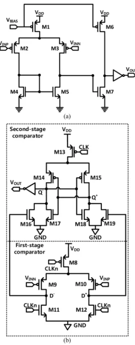
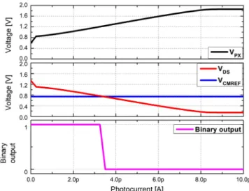
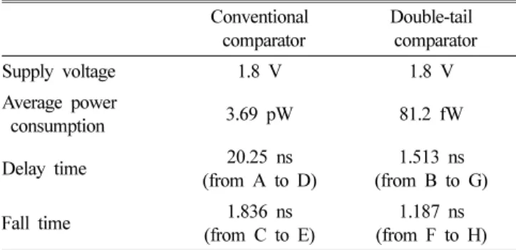
In this paper, we propose a complementary metal-oxide semiconductor (CMOS) binary image sensor with a gate/body-tied (GBT) p-channel metal-oxide-semiconductor field-effect transistor (PMOSFET)-type photodetector using a double-tail comparator for high- speed and low-power operations. The GBT photodetector is based on a PMOSFET tied with a floating gate (n+ polysilicon) and a body that amplifies the photocurrent generated by incident light. A double-tail comparator compares an input signal with a reference voltage and returns the output signal as either 0 or 1. The signal processing speed and power consumption of a double-tail comparator are supe- rior over those of conventional comparator. Further, the use of a double-sampling circuit reduces the standard deviation of the output voltages. Therefore, the proposed CMOS binary image sensor using a double-tail comparator might have advantages, such as low power consumption and high signal processing speed. The proposed CMOS binary image sensor is designed and simulated using the standard 0.18 µm CMOS process.

Keywords: CMOS image sensor, GBT PMOSFET-type photodetector, Binary image sensor, Double-tail comparator

1. INTRODUCTION

An image sensor detects incident light and converts it into a digital signal. The two main types of image sensors are the charge-coupled device (CCD) sensor and the CMOS image sensor (CIS). The CCD image sensor transmits the electrons generated by incident light to an integrated amplifier. The CIS converts the electrons generated by incident light into voltage in each source follower. The disadvantage of the CIS is the presence of dark current in the photodiode and readout noise. The noise issues in CISs are improved by the development of process technology.

The CIS has advantages such as high speed, low cost, and high integration as compared with CCD image sensors. Currently, CISs are used in various applications, such as smartphones and wearable devices. Furthermore, the proposed CMOS binary image sensor is expected to be used in applications such as text recognition, fingerprint detection, motion detection, and barcoding

[1-5].

The p-n junction photodiode, bipolar junction transistor (BJT) photodiode, and avalanche photodiode (APD) are used in the photodetector of CISs. A BJT photodiode requires a large area [6].

An APD exhibits a high sensitivity. However, it requires a high reverse bias voltage [7]. The p-n junction photodiode exhibits a low sensitivity. Among these photodetectors, the p-n junction photodiode is manufactured using standard CMOS processes and is used in conventional CISs. The proposed gate/body-tied (GBT) p-channel metal-oxide-semiconductor field-effect transistor (PMOSFET)-type photodetector exhibits a high sensitivity and occupies a small area [8-10].

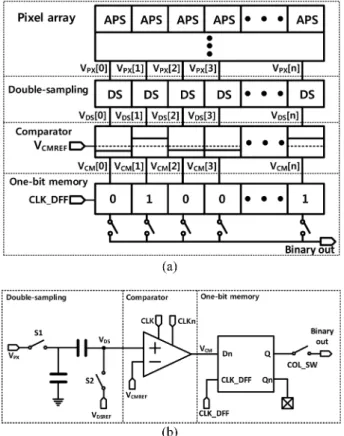
There are various types of binary image processing methods. A comparator compares the output signal of an active pixel sensor (APS) with a binary signal and performs high-speed signal processing [11-12]. The pixel from the input video image and the signal voltage of the APS are synchronized and input to a binary processing device [13]. A quantum image sensor using an optimized 1-bit analog-to- digital converter (ADC) is a binary image sensing system [14]. The proposed double-tail comparator converts the output signal of an APS to a binary signal [15-17].

In this paper, we propose a CMOS binary image sensor using a GBT PMOSFET-type photodetector and a double-tail comparator for high-speed and low-power operations. The sensitivity of a GBT PMOSFET-type photodetector is higher than that of a conventional p-n junction diode. To improve the signal School of Electrical Engineering, Kyungpook National University

Sangyeok 3-dong, Buk-gu, Daegu, 41566, KOREA.

+

Corresponding author: [email protected]

(Received: Mar. 13, 2020, Revised: Mar. 29, 2020, Accepted: Mar. 30, 2020)

This is an Open Access article distributed under the terms of the Creative Commons Attribution Non-Commercial License(https://creativecommons.org/

licenses/by-nc/3.0/) which permits unrestricted non-commercial use, distribution,

and reproduction in any medium, provided the original work is properly cited.

(2)

processing speed and power consumption of the GBT PMOSFET- type photodetector, a double-tail comparator is used. The proposed CMOS binary image sensor is designed and simulated using a standard 0.18 μm CMOS process.

2. OPERATING PRINCIPLES

2.1 GBT PMOSFET-type photodetector of an APS Fig. 1 (a) shows the schematic of an APS with a GBT PMOSFET-type photodetector. The APS comprises three NMOSFETs and a GBT PMOSFET-type photodetector. The floating gate (n+ polysilicon) of the GBT PMOSFET-type photodetector is tied with the body (n-well). M1 functions as a source follower for amplifying the floating-diffusion (FD) node voltage, M2 resets the FD node to V

PXREF

, and M3 performs the row selection. The incident light penetrates through the gate of the GBT PMOSFET-type photodetector and generates electron-hole pairs (EHPs) in the depletion layer of the PMOSFET. The

generated holes are drawn into the FD node through the channel, and the electrons decrease the voltage of the gate and body. The GBT PMOSFET-type photodetector amplifies the photocurrent generated by incident light. Therefore, the GBT PMOSFET-type photodetector exhibits a high sensitivity.

Fig. 1 (b) shows a cross-section of the GBT PMOSFET-type photodetector. Except in the photodiode region, a metal shielding layer is used to block light.

2.2 CMOS binary image processing

Fig. 2 (a) shows the architecture of the CMOS binary image sensor processing system and Fig. 2 (b) shows the schematic of a unit column readout circuit. The proposed CMOS binary image sensor comprises a pixel array, double-sampling circuit, comparator, and 1-bit memory. The column-parallel readout circuits for binary image processing comprise a double-sampling circuit, comparator, and 1-bit memory.

The pixel output voltage (V

PX

) is fed into the double-sampling circuit and converted to a double-sampling voltage (V

DS

). In CISs, one component of the fixed-pattern noise (FPN) is performance variation of each pixel amplifier. The FPN of V

PX

is removed using double-sampling. V

DS

is compared with the reference

Fig. 1. (a) Schematic of an APS with a GBT PMOSFET-type pho- todetector and (b) cross-section of a GBT PMOSFET-type photodetector.

Fig. 2. (a) Architecture of the CMOS binary image-sensor processing

system and (b) schematic of unit column readout circuit.

(3)

voltage of the comparator (V

CMREF

). If V

DS

is higher than V

CMREF

, the output of the comparator (V

CM

) is high (i.e., 1), and if V

DS

is lower than V

CMREF

, V

CM

is low (i.e., 0). V

CM

is a digital signal and is stored in the 1-bit memory and then sequentially output. V

PX

, which stores the information of the incident light, is fed into the column-parallel readout circuits and converted to a binary output.

The CMOS binary image sensor signal processing circuits are simpler than the CIS signal processing circuits, thus rendering high-speed and low-power operation in these sensors possible.

Fig. 3 shows the timing diagram of the CMOS binary image sensor. The column-parallel readout circuits are used in the proposed CMOS binary image sensor. Pixels of the same row are simultaneously sampled. The timing diagram shows the unit-row operation. A unit-row operation comprises the sampling time and readout time.

When the selected voltage of the APS (V

SEL

in Fig. 1 (a)) is high, a row in the pixel array is selected. The reset voltage of the APS (V

RST

in Fig. 1 (a)) resets the FD node. V

SEL

and V

RST

are controlled using a vertical scanner. S1 and S2 are switches in the double-sampling circuit. The output voltage and reset voltage of each pixel in each column are sampled. When the CLK signal falls, the comparator compares V

DS

in Fig. 2 with V

CMREF

. V

CM

in Fig. 2 is a binary signal and is determined using the comparator.

When COL_SW in Fig. 2 is switched on, the stored signal in the 1-bit memory is output. In each column, COL_SW is controlled using a horizontal scanner that is sequentially operated. Therefore, the binary output in each column is sequentially read.

2.3 Double-tail comparator

Fig. 4(a) shows the schematic of a conventional comparator. A conventional comparator operates continuously based on the bias

voltage (V

BIAS

). Two input signals (V

INP,

V

INN

) are compared continuously using a comparator. When V

INP

is smaller than V

INN

, V

OUT

is low (0). A conventional comparator is not suitable for CMOS binary image sensors owing to its disadvantage of higher power consumption.

Fig. 4(b) shows the schematic of the double-tail comparator.

When the clock signal changes, the double-tail comparator compares V

INP

with V

INN

, and current simultaneously flows in the circuit. Therefore, the double-tail comparator reduces unnecessary power consumption. The CLKn signal is an inverted clock signal.

V

INP

is the double-sampling voltage with information of the Fig. 3. Timing diagram of the CMOS binary image sensor.

Fig. 4. Schematic of (a) the conventional comparator and (b) the

double-tail comparator.

(4)

incident light. V

INN

is a fixed reference voltage. D+ and D− are output signals of the first-stage comparator. Q+ and Q− are output signals of the second-stage comparator. When the CLK signal starts to fall and CLKn starts to rise, the double-tail comparator compares V

INP

and V

INN

.

During the first-stage comparator operation, the voltages of the D+ and D− nodes fall from V

DD

to GND. If V

INP

is smaller than V

INN

, the current through transistor M8 flows through transistor M10. Simultaneously, the voltage of D+ falls faster than the voltage of D−. D+ and D− are input signals of the second-stage comparator. The transistors M15, M16, M17, M18, and M19 are switched off and the transistors M13 and M14 are switched on.

The current through transistor M13 flows through transistor M14.

Therefore, the voltage of the Q− node increases. When V

INP

is smaller than V

INN

, the output signal of the double-tail comparator, with the voltage at the Q− node inverted, is determined to be low (0).

Both conventional and double-tail comparators can convert an analog signal to a binary signal. The conventional comparator operates continuously causing current to flow through the circuit.

However, the double-tail comparator operating at the clock signal is changed. Furthermore, its signal processing speed is faster than that of a conventional comparator. Therefore, a double-tail comparator is better suited for the proposed CMOS binary image sensor.

3. SIMULATION RESULTS

The proposed CMOS binary image sensor was evaluated using the Cadence Spectre simulator. In this simulation, light intensity is represented as a photocurrent and the exposure time is 500 μs.

3.1 Variation in the signal voltage

Fig. 5 shows the simulation results for the variation in signal voltage with the photocurrent. V

PX

is the pixel output voltage and is determined by the photocurrent. If the photocurrent is approximately 9 pA, V

PX

is saturated. V

PX

is converted to V

DS

, which is the double-sampling voltage. V

CMREF

is the reference voltage in the comparator and is 0.74 V. If V

DS

is larger than V

CMREF

, the binary output is determined to be high (1), and if V

DS

is lower than V

CMREF

, the binary output is determined to low (0).

Furthermore, if the photocurrent is larger than 3.5 pA, the binary output is low (0).

3.2 FPN reduction using double-sampling circuit Table 1 shows the results of Monte Carlo simulations prior and subsequent to voltage double-sampling. The double-sampling circuit converts the pixel output voltage to the double-sampling voltage and reduces the FPN of the pixel output voltage. The voltages are sampled 1000 times in the Monte Carlo simulation.

The mean values of the pixel output voltage and double-sampling voltage are 1.5901 V and 0.8509 V, respectively. The standard deviations of the pixel output voltage and double-sampling voltage are 25.31 mV and 3.28 mV, respectively. The standard deviation of the voltage was reduced by approximately 87%, by using double-sampling.

Fig. 6 shows the histogram of the Monte Carlo simulation. The X-axis of the histogram represents the deviation from the mean value and the Y-axis represents the number of samples. The double-sampling voltage is distributed closer to the mean than the pixel voltage, thus confirming the reduction in deviation using double-sampling.

Fig. 5. Simulation results for the variation in signal voltage with the photocurrent.

Table 1. Results of the Monte Carlo simulations prior and subsequent to voltage double-sampling.

The pixel output voltage

The double-sampling voltage

Number of samples 2000 2000

Mean 1.59015 [V] 0.8509 [V]

Standard Deviation 25.31 mV 3.28 mV

(5)

3.3 Operation of each comparator and power consumption

Fig. 7 shows the simulation results of the output voltages and currents from a conventional comparator and a double-tail comparator. In this simulation, the photocurrent is 4 pA and V

CMREF

is 0.74 V, and the conventional comparator operates continuously. When the switch of double-sampling is turned on,

V

DS

changes. For V

DS

≤ V

CMREF

, the output voltage of the conventional comparator is determined to be low (0). After double-sampling, V

DS

and V

CMREF

are fed into the double-tail comparator. The double-tail comparator compares V

DS

with V

CMREF

, when CLK, which is the clock signal, falls.

The current of a conventional comparator flows continuously.

However, the current of a double-tail comparator flows only during the operation of the comparator. Thus, power consumption is improved using a double-tail comparator as compared to a conventional comparator.

Table 2 shows the comparison of the comparators. The supply voltage for each comparator is 1.8 V. In Fig. 7, for 500 ns operation, the power consumption of the conventional comparator is 3.69 pW, and while the power consumption of the double-tail comparator is 81.2 fW. Therefore, if a conventional comparator is replaced by a double-tail comparator, the power consumption could be reduced by approximately 97.8%.

3.4 Delay time and fall time of the comparators In Fig. 7, the delay time of the conventional comparator, which is 20.25 ns, is the time taken by the current to travel from point A to point D. The delay time of the double-tail comparator, which is 1.513 ns, is the time taken by the current to travel from point B to point G. The fall time of the conventional comparator, which is 1.836 ns, is the time taken by the current to travel from point C to point E, while the fall time of the double-tail comparator, which is 1.187 ns, is the time taken by the current to travel from point F to point H. By using the double-tail comparator, the delay and fall times are reduced by approximately 92.53% and 35.35%, respectively, compared to those obtained using a conventional comparator.

Fig. 8 shows the simulation results for the variation in the delay and fall times with the photocurrent. If the photocurrent is lesser than 3.5 pA, V

DS

is lesser than 0.74 V and the binary output is high (1). In this case, there is no delay time and fall time.

Fig. 6. Histogram of Monte Carlo simulations.

Fig. 7. Simulation results of the output voltages and currents from a conventional comparator and a double-tail comparator.

Table 2. Comparison of the comparators (simulation results of Fig. 7).

Conventional comparator

Double-tail comparator

Supply voltage 1.8 V 1.8 V

Average power

consumption 3.69 pW 81.2 fW

Delay time 20.25 ns

(from A to D)

1.513 ns (from B to G)

Fall time 1.836 ns

(from C to E)

1.187 ns

(from F to H)

(6)

In Fig. 8, when the photocurrent is 3.5 pA, V

DS

is closest to 0.74 V. This case exhibits the longest delay and fall times in the simulation. The delay time and fall time of a conventional comparator depend on the photocurrent. However, the delay and fall times of a double-tail comparator are constant. The delay and fall times of a double-tail comparator are unaffected by the difference in the two input voltages. Therefore, a double-tail comparator is more suitable for high-speed operations than a conventional comparator.

4. CONCLUSIONS

A CMOS binary image sensor based on a GBT PMOSFET-type photodetector is proposed for high-speed and low-power operation. The power consumption is reduced by approximately 97.8% when a double-tail comparator is used, and the delay and fall times improve compared with conventional comparators. The double-sampling circuit reduces the standard deviation of the output voltages. Therefore, the proposed CMOS binary image sensor using a double-tail comparator might have advantages, such as low power consumption and high signal processing speed.

ACKNOWLEDGMENT

This research was supported by the Basic Science Research Program through the National Research Foundation of Korea (NRF) funded by the Ministry of Education (2018R1D1A3B07049952), and the Integrated Circuit Design Education Center (IDEC) in Korea.

REFERENCES

[1] E. R. Fossum and S. Member, “CMOS Image Sensors : Electronic Camera-On-A-Chip”, IEEE Trans. Electron Devices, Vol. 44, No. 10, pp. 1689-1698, 1997.

[2] S. Mehta, A. Patel, and J. Mehta, “CCD or CMOS Image sensor for photography”, 2015 Int. Conf. Commun. Signal Process. ICCSP 2015, pp. 291-294, Melmaruvathur, India, 2015.

[3] B. S. Carlson, “Comparison of Modern CCD and CMOS Image Sensor Technologies and Systems for Low Reso- lution Imaging”, Proc. IEEE Sens., Vol. 1, No. 1, pp. 171- 176, 2002.

[4] M. Bigas, E. Cabruja, J. Forest, and J. Salvi, “Review of CMOS image sensors”, Microelectron. J., Vol. 37, No. 5, pp. 433-451, 2006.

[5] B. Luo, L. Yan, and F. Yang, “Research of noise sup- pression for CMOS image sensor”, 2010 Int. Conf. Meas.

Technol. Mechatron. Autom. ICMTMA 2010, Vol. 2, pp.

1100-1103, Changsha City, China, 2010.

[6] N. Tanaka, T. Ohmi, and Y. Nakamura, “A novel bipolar imaging device with self noise reduction capability”, IEEE Trans. Electron Devices, Vol. 36, No. 1, pp. 31-38, 1989.

[7] A. Rochas, A. R. Pauchard, P. A. Besse, D. Pantic, Z. Prijic, and R. S. Popovic, “Low-noise silicon avalanche photo- diodes fabricated in conventional CMOS technologies”, IEEE Trans. Electron Devices, Vol. 49, No. 3, pp. 387-394, 2002.

[8] W. Zhang and M. Chan, “A high gain N-Well/Gate tied PMOSFET image sensor fabricated from a standard CMOS process”, IEEE Trans. Electron Devices, Vol. 48, No. 6, pp.

1097-1102, 2001.

[9] H. H. Lee, S. H. Jo, M. Bae, B. S. Choi, J. Kim, H. K. Lyu, and J. K. Shin, “Highly sensitive gate/body-tied metal- oxide-semiconductor field-effect transistor-type photode- tector with wavelength-selective metal grid structure using standard complementary metal-oxide-semiconductor tech- nology”, Sens. Mater., Vol. 27, No. 1, pp. 135-142, 2015.

[10] B. S. Choi, S. H. Kim, J. Lee, C. W. Oh, S. H. Seo, and J.

K. Shin, “Complementary metal oxide semiconductor image sensor using gate/body-tied P-channel metal oxide semiconductor field effect transistor-type photodetector for high-speed binary operation”, Sens. Mater., Vol. 30, No. 1, pp. 129-134, 2018.

[11] B.-S. Choi, S.-H. Jo, M. Bae, J. Kim, P. Choi, and J.-K.

Shin, “High-Speed CMOS Binary Image Sensor with Gate/

Body-Tied PMOSFET-Type Photodetector”, J. Sens. Sci.

Technol., Vol. 23, No. 5, pp. 332-336, 2014.

[12] J. Lee, B.-S. Choi, D. Seong, J. Lee, S.-H. Kim, J. Lee, J.- K. Lee, and P. Choi, “CMOS Binary Image Sensor with Gate / Body-Tied PMOSFET-Type Photodetector for Low- Power and Low-Noise Operation”, J. Sens. Sci. Technol., Vol. 27, No. 6, pp. 362-367, 2018.

[13] B. Zhang, K. Mei, and N. Zheng, “Reconfigurable pro- cessor for binary image processing”, IEEE Trans. Circuits Syst. Video Technol., Vol. 23, No. 5, pp. 823-831, 2013.

[14] S. Masoodian, A. Rao, J. Ma, K. Odame, and E. R. Fossum, Fig. 8. Simulation results for variation in delay and fall times with

the photocurrent.

(7)

“A 2.5 pJ/b Binary Image Sensor as a Pathfinder for Quanta Image Sensors”, IEEE Trans. Electron Devices, Vol. 63, No.

1, pp. 100-105, 2016.

[15] D. Schinkel, E. Mensink, E. Klumperink, E. Van Tuijl, and B. Nauta, “A double-tail latch-type voltage sense amplifier with 18ps setup+hold time”, Dig. Tech. Pap. - IEEE Int.

Solid-State Circuits Conf., pp. 314-316, San Francisco, CA, USA, 2007.

[16] S. Chaudhari and M. Pawar, “Design of efficient double tail comparator for low power”, 2015 Int. Conf. Commun. Sig- nal Process. ICCSP 2015, pp. 1782-1785, Melmaruvathur, India, 2015.

[17] S. Mashhadi, “Analysis and Design of a Low-Voltage Low-

Power Double-Tail Comparator”, IEEE Trans. VLSI Syst.,

Vol. 22, No. 2, pp. 343-352, 2014.

수치

Fig. 2 (a) shows the architecture of the CMOS binary image sensor processing system and Fig
Fig. 3 shows the timing diagram of the CMOS binary image sensor. The column-parallel readout circuits are used in the proposed CMOS binary image sensor
Fig. 5 shows the simulation results for the variation in signal voltage with the photocurrent
Table 2 shows the comparison of the comparators. The supply voltage for each comparator is 1.8 V

참조

관련 문서