반도체디스플레이기술학회지 제19권 제3호(2020년 9월)
Journal of the Semiconductor & Display Technology, Vol. 19, No. 3. September 2020.
19
Thermal Evaporation 증발원 개발 및 응용에 관한 연구
김관도
* †
* †
평택대학교 융합소프트웨어학과A Study on the Development and Application of Thermal Evaporation Source
Kwan-Do Kim
*†
* †
Dept. of Convergence Software, PyeongTaek UniversityABSTRACT
The thermal evaporation source is used to prepare thin films by physical vapor deposition. Materials of metals, organic materials, were tested and explained for thermal evaporation experiments. The developed effusion cell performance depends on the type of deposition material, the size of the crucible, the performance of the reflector, etc.
and the proper conditions were found by producing, comparing and analyzing several sets of effusion cell to quantitatively evaluate the performance of the cell. The effusion cell for thermal evaporation source is used to prepare thin films of Ag, Cu, Mg.
Key Words : Physical Vapor Deposition, Thermal Evaporation, Effusion cell, Thin Film
1. 서 론1
진공 증착 부품은 디스플레이 소자나 반도체 소자 제 작 시 박막 증착에 필수적으로 사용되는 핵심장치이다.
이 장치들은 불순물 유입이 최대한 배제되어야 하는 디 스플레이 소자나 반도체 소자의 최적 성능을 구현하기 위해 필수적이다 [1-10]. 국내외적으로 장비 및 부품업체 들이 진공 증착 장비를 개발하고 있으나, 아직까지 규격 화되어 있지 않으며 양산장비에 적용될 수 있는 수준의 안정된 제품이 상용화되어 있지 않은 상태이다.
진공 증착 또는 진공 증발이란 고진공의 챔버(chamber) 내에 증착될 대상 물질을 놓고 전류 등에 의해 소스 물질 을 가열함으로써 그 입자를 증발시키고, 이를 상대적으로 차가운 기판 등의 표면에 응축하여 박막을 형성하는 증 착 방법으로서, 반도체 제조 공정에서 웨이퍼 표면에 특 정 물질로 이루어지는 박막을 형성하거나, 박막형 태양전
† E-mail: [email protected]
지 또는 대형 평판 디스플레이 장치의 제조에 있어서 Glass 기판 등의 표면에 원하는 물질로 이루어지는 박막 을 형성하는 데에 널리 이용되고 있다[11-16]. 증착 박막 균일도는 crucible의 입구의 크기와 모양에 따라 분자선 빔 의 퍼짐이 결정되며 이에 따라 증발원과 기판과의 거리 를 조절하는 방법이 있으며 증착률 균일도는 증발원의 온도를 일정하게 유지하고, 증발형 물질인 경우는 용융 상태의 증발물질 자체의 열전도 및 대류에 의해 비교적 쉽게 균일도가 확보되나, 승화형 물질의 경우는 crucible의 상부와 하부의 온도차를 줄임으로써 균일도를 확보할 수 있다. Filament는 증발물질과 증발원의 구조에 따라 다양한 형태로 만들어지며, 이에 대한 정확한 형상은 선택적으로 정해진다. filament에서 발생한 열을 가두는 열차단 반사판 은 filament에서 발생한 열을 차단하여 내부로 모아주는 역할을 함으로써 crucible의 온도 균일성을 보장하게 된다.
이 반사판에는 Ta, Mo, W 등이 사용되며, 반사판의 열차단 효과는 반사판을 몇 겹으로 제작하느냐에 의해 결정되며, 이는 crucible의 상하부 온도차, filament와 crucible의 온도차
김관도
반도체디스플레이기술학회지 제19권 제3호, 2020 20
이, 열효율 등을 결정짓는 요소이다.
2. Thermal evaporation을 이용한 증착 실험
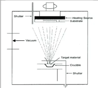
증착 재료를 증발시키려면 충분한 vapor가 발생되도록 증착 재료를 가열해 줄 수 있는 장치가 필요하다. 이렇게 증착 재료의 vapor를 발생시켜주는 장치를 evaporation source라 한다. Source 용량의 한계는 증착 재료를 균일한 온도로 가열하는데 한계가 있어 동일한 crucible을 여러 개 순서대로 사용하는 방법 등으로 해결해 나가고 있다. 또 한 crucible 입구의 막힘 현상이나 crucible주변 또는 기판에 증착 재료가 튀는 현상도 단점으로 지적되고 있다. 이는 crucible 입구와 몸체 및 증착 재료의 온도 차이, 증착 재 료의 순도 및 수분 함유량 등에 의한 것인데 이를 해결하 기 위하여 순도가 높고 증착 특성이 좋은 증착 재료를 개 발하는 것과 함께 crucible의 구조를 변경하거나 source에 사용하는 열선의 재질 및 제작 방법을 변경하여 온도 편 차를 줄이는 방법을 사용하고 있다. 개발된 상향식 점진 공 증발원의 성능 평가는 증착 물질의 종류, crucible의 크 기, 반사판의 성능 등에 의해 좌우되며 증발원의 성능을 정량적으로 평가하기 위해 여러 set의 증발원을 제작하여 비교, 분석함으로써 적정 조건을 찾을 수 있었다. 개발된 effusion cell을 OMBD(Organic Molecular Beam Deposition) 장비 에 장착하여 온도 튜닝 및 안정화 테스트 실험을 한 뒤 metal과 유기물에 대해서 증착 실험을 진행하였다. OMBD 장비는 유기박막 소자의 핵심요소인 저분자량 유기반도 체 물질과 금속을 진공 증착하는 장비로서, 진공 증발원
Fig. 1. OMBD(Organic Molecular Beam Deposition) process chamber with thermal evaporation source.
을 통해 자유로운 증착 속도 조절 및 증착 속도 안정화가 가능하다. 또한 기판의 적절한 온도 조절 및 유지가 가능 하다. Fig. 1에 thermal evaporation source가 장착된 OMBD 장비 의 개략도 (schematic diagram)을 도식적으로 나타내었다.
증착 실험을 진행하기 위해Process Chamber의 진공도를 TMP(Turbo Molecular Pump)를 사용하여 1x10
-6
Torr 이하를 유 지하였다. Fig. 2와 Fig. 3은 개발된 증발원을 사용하여 5 x 5 cm 실리콘 기판에 Ag와 Cu박막을 thermal evaporation방법으 로 증착시키고 HR FE-SEM(JEOL JSM-7401F)을 이용하여 단면 및 표면 사진을 찍은 것이며 Spectroscopic Ellipsometry (J. A. Woollam, M2000) 및 주사전자현미경(Scanning Electron Microscope, SEM)으로 측정한 박막 두께의 편차는 5 % 이 내로 균일하였다.(a) (b)
Fig. 2. Thermal evaporation deposited Ag thin film HR FE- SEM image. (a) cross section (b) top-view image.
(a) (b)
Fig. 3. Thermal evaporation deposited Cu thin film HR FE- SEM image. (a) cross section (b) top-view image.
Fig. 4는 thermal evaporation으로 증착시킨 Ag, Cu, Mg에 대 하여 cell 온도에 따른 desposition rate를 그래프로 각각 나타 낸 것이다.Cu 박막 증착의 경우 Eurotherm controller를 사용 하여 30℃/min의 rate로 온도를 올렸으며 1000℃에서부터 초기 evaporation이 일어나기 시작하였다. 온도가 증가함에 따라 deposition rate가 증가하고 있음을 알 수 있다. 1400℃에 서 증착 실험을 진행하였으며, deposition rate는 1 Å/sec으로 일정하게 유지되었으며 rate 편차는 0.1 Å/sec로 일정하였 다. 증착 공정이 진행되는 동안 온도편차도 ±0.1℃ 이내로
Thermal Evaporation 증발원 개발 및 응용에 관한 연구
Journal of KSDT Vol. 19, No. 3, 2020 21
(a)
(b)
(c)
Fig. 4. Deposition rate vs. cell temperature. (a) Ag (b) Cu (c) Mg.
일정하게 유지되었다.
Table 1에 thermal evaporation을 이용한 박막 증착 실험에 사용된 증착 물질의 density(g/cm
3
)와 Z-ratio 값을 나타내 었다.Table 1. Material parameter (Density and Z-ratio)
Formula Density(g/cm 3 ) Z-ratio Material Name
Ag 10.5 0.529 Silver
Cu 8.93 0.437 Copper
Mg 1.74 1.610 Magnesium
3. 결과 및 고찰
증발원에 의한 증착은 다음과 같이 크게 세 단계를 거 쳐 이루어지며 그 과정은 다음과 같다. 첫째, 저항가열에 의해 발생한 열에너지에 의해 가스 상태로 기화되는 과 정이다. 둘째, 챔버 내의 고진공 중에서 증발체가 증발원 과 기판 사이를 통과하여 이동하는 과정이다. 증발원에서 증발한 입자는 챔버 내에서 이동하게 되며 이때 증발한 입자가 충돌하지 않고 직진할 수 있는 거리를 평균자유 행로라고 한다. 셋째, 기판에 도달한 기체상의 증발체가 응축하여 핵생성과 성장을 거쳐 증착층을 형성하는 과정 이다. 증착층을 형성하는 과정에서 박막 성장 방법에 관
(a)
(b)
Fig. 5. High Resolution FE-SEM EDS(Energy Dispersive Spectroscopy) spectrum of deposited by thermal evaporation (a) Ag film and (b) Cu film.
김관도
반도체디스플레이기술학회지 제19권 제3호, 2020 22
한 이론을 따른다. Evaporation 방식으로 증착 제조한 박막 의 성질은 기판의 온도, 기판 사이의 거리, 증착 전류 및 압력 등에 따라 달라지며 증착층은 증기입자가 거의 직 선으로 이동되어 증착되므로 기판에 수직한 형태의 조직 을 형성하며 높은 비등방성을 가지게 된다. 점진공 증발 원은 하부에 고정된point source를 가열하여 증착 물질의 vapor를 발생시키고 분출시켜 증착 공정을 수행하는 방법 이다. 이때 균일한 박막을 얻기 위해서 source의 구조, source와 기판 사이의 거리, 각도 등의 조건을 만족하여야 한다. 때문에 기판의 크기가 커질수록 거리를 멀리 하거 나 기판을 회전시키는 등의 단점이 있다. 본 실험에서는 개발된 effusion cell을 사용하여 Ag와 Cu를 증착 물질로 thermal evaporation을 진행하였으며 Fig. 5에 HR FE-SEM EDS(Energy Dispersive Spectroscopy) 조성 분석을 진행한 결과 Ag와 Cu 박막이 잘 증착되었음을 확인하였다.
4. 결 론
본 연구에서는 점진공 증발원을 이용하여 금속의 증발 특성을 연구하였다. 개발된 effusion cell을 사용하여 thermal evaporation에 의한 금속 증착(Ag, Cu, Mg) 실험에 적용하였 으며 디스플레이 소자나 반도체 소자의 전극과 같은 metal 박막을 형성하는데 있어 최적 성능을 구현하는데 활용 가능함을 알 수 있었다. 진공 증발원 관점에서 증착 재료의 사용효율 개선, 대형 기판에 균일하고 고속 증착 이 가능한 thermal evaporation 증발원의 최적화를 위한 지속 적인 개발이 필요하다.
참고문헌
1. B. D. Yao, Y.F.Chan, and N. Wang, “Formation of ZnO nanostructures by a simple way of thermal evaporation”, Applied Physics Letters, vol. 81, No. 4, pp. 757-759, 2002.
2. Sung Hoon Jun and Eung Ki Lee, “DSMC Simulation of a Point Cell-source for OLED Deposition Process”, Journal of the Semiconductor & Display Technology, Vol. 9, No. 3, pp. 11-16, 2010.
3. Gi Chung Kwon et al, “Study of ALD Process using the Line Type Plasma Source”, Journal of the Semiconductor
& Display Technology, Vol. 15, No. 4, pp. 33-35, 2016.
4. Eung Ki Lee, “Study on Optimization of the Vacuum Evaporation Process for OLED”, Journal of the Semiconductor & Display Equipment Technology, Vol.
7, No. 1, pp. 35-40, 2008.
5. Nam Ihn Cho and Min Chul Kim, “The Formation
Technique of Thin Film Heaters for Heat Transfer Components”, Journal of the Semiconductor & Display Equipment Technology, Vol. 2, No. 4, pp. 31-35, 2003.
6. Youngcheol Joo et al, “Thermal Performance Analysis of Circular Source for OLED Vapor Deposition”, Journal of the Semiconductor & Display Equipment Technology, Vol. 6, No. 4, pp. 39-42, 2007.
7. Eung Ki Lee, “Three Dimensional Direct Monte Carlo Simulation on OLED Evaporation Process”, Journal of the Semiconductor & Display Equipment Technology, Vol. 8, No. 4, pp. 37-42, 2009.
8. Heon Lee, Sunghoon Hong, Kiyeon Yang, and Kyungwoo Choi, “Fabrication of Nano-sized Resist Patterns on Flexible Plastic Film using Thermal Curing Nano-imprint Lithography,” Microelectronic Engineering, Vol. 83, pp. 323-327, 2006.
9. Michael S. Arnold, Gregory J. McGraw, Stephen R.
Forrest, and Richard R. Lunt, “Direct Vapor Jet Printing of Three Color Segment Organic Light Emitting Devices for White Light Illumination,” Applied Physics Letters, Vol. 92, No. 5, pp. 3301, 2008.
10. Sang Chul Lim, Seong Hyun Kim, Hye Yong Chu, Jung Hun Lee, Jeong-Ik Lee, Ji Young Oh, Dojin Kim, and Taehyoung Zyung, “New Method of Driving OLED with an OTFT,” Synthetic Metals, Vol. 151, pp. 197-201, 2005.
11. Milton S. Hess and John F. Mikosky, “Vapor Deposition of Platinum using cw Laser Energy,” Journal of Applied Physics, Vol. 43, No. 11, pp. 4680-4683,1972.
12. Eungki Lee, “Simulation of the Thin-film Thickness Distribution for an OLED Thermal Evaporation Process,”Vacuum, Vol. 83, pp. 848-852, 2009.
13. Spencer E. Olson and Andrew J. Christlieb, “Gridless DSMC,” Journal of Computational Physics, Vol. 227, pp.
8035-8064, 2008.
14. J. B. Anderson and J. B. Fenn, “Velocity Distributions in Molecular Beams from Nozzle Sources,” The Physics of Fluids, Vol. 6, No. 5, pp.780-787, 1965.
15. P. S. Prasanth and Jose K. Kakkassery, “Molecular Models for Simulation of Rarefied Gas Flows using Direct Simulation Monte Carlo Method,” Fluid Dynamics Research, Vol. 40, pp. 233-252, 2008.
16. Eung Ki Lee, “Evaporation Process Modeling for Large OLED Mass-fabrication System”, Journal of the Semiconductor & Display Equipment Technology, Vol.
5, No. 4, pp. 29-34, 2006.
접수일: 2020년 8월 6일, 심사일: 2020년 8월 18일, 게재확정일: 2020년 8월 27일