https://doi.org/10.7840/kics.2017.42.4.798
대역폭 향상을 위한 소형 MCR 구조를 갖는 Ultra-Wide Band 안테나 설계
이람 나담, 김 영 진°
Design of Ultra-Wide Band Antenna with Compact MCR Structure for BW Enhancement
Iram Nadeem, Young-Jin Kim°
요 약
본 논문은 슬롯이 삽입된 접지, 수정된 급전선 및 서로 다른 반지름을 갖는 원형 링 구조의 패치 안테나를 제 시한다. 안테나의 크기는 15 × 12 ㎟이며, 전체 면적 180 ㎟ 및 전기적 치수 0.14λ × 0.12λ(초단 주파수)를 갖는 다. 제안된 안테나는 3.1 ㎓ ∼ 12.3 ㎓ 대역을 포함하며, 대역폭 비 4.13:1, 비 대역폭 122%, 반사계수 최대 -38
㏈의 결과를 보인다. 소형화된 크기를 증명하기 위해 대역폭 크기 비율이 계산되었다. 공급 라인에 삽입 된 얇은 슬롯은 전체 주파수 대역에서 우수한 임피던스 정합을 제공한다. 제안된 안테나의 시뮬레이션은 반사 계수≤-10
㏈, VSWR 2:1, 방사 패턴 및 군지연 (ns)을 시뮬레이션 결과로 제시하였다. 제안된 안테나는 우수한 임피던스 정 합 및 매우 작은 크기의 장점을 보이며, 대역폭 향상 및 UWB 단거리 고속 무선통신을 제공한다.
Key Words : Multi Circular Ring (MCR), Ultra-wide Band (UWB), Slotted ground (SG), Bandwidth dimension ratio (BDR)
ABSTRACT
This paper presents a low profile multi circular ring with different radius, patch antenna with modified feed line and slotted ground. The size of the antenna is 15 × 12 ㎟, having electrical dimensions of 0.14λ × 0.12λ (at lower initial frequency) and footprints of 180 ㎟. The proposed antenna covers 3.1 to 12.3 ㎓, reflection coefficient up to -38 ㏈ with Bandwidth ratio of 4.13:1 and fractional Bandwidth of 122%. Bandwidth dimension ratio has been calculated (which is 6246) as a proof for compact size. Thin slots introduced on the feed line provide good impedance matching for whole frequency band. Numerical simulations of the proposed antenna are reported in terms of reflection coefficient ≤ -10 ㏈ , vswr 2:1 , radiation pattern and group delay (ns). The proposed antenna has advantage of very small size along with better impedance match that provides a practical approach to realize it for BW enhancement and UWB applications.
First Author : Chosun University Department of Information and Communication Engineering, engineer,[email protected], 학생회원
° Corresponding Author : chosun college of science & technology, [email protected], 정회원
논문번호:KICS2017-03-064, Received March 6, 2017; Revised March 17, 2017; Accepted March 23, 2017
Ⅰ. Introduction
The Ultra-wide band technology (3.1 ㎓ to 10.6
㎓) has grabbed much more attention because of
increasing demand of multi band compact size antenna for wireless communication applications. It is a potentially revolutionary approach to wireless communication applications and growing very
rapidly. Currently very high speed, high precision radars are offering promising technology for imaging systems. Since 2002, the FCC (Federal commission of communication, USA) allocated as unlicensed frequency band as Ultra-wide band technology ranging between 3.1 ㎓ to 10.6 ㎓. In Europe (ETSI 2015) has divided this band into two further bands according to its applications. The commission has defined rules and regulations regarding bandwidth, power transmission requirements and frequency bands. UWB can be described as any wireless scheme showing fractional bandwidth greater than 20 % or 500 ㎒ of absolute bandwidth. In other words, UWB technology has gained lots of attention from last few decades because of its ability to optimize the performance of the existing systems and open new doors for internet of thing (IoT) applications. The attractive provide wide bandwidth, high data rate, interference mitigation and low power consumption with location and tracking. It is commonly referred as signals or systems that have very large absolute bandwidth which offers certain advantages with respect to signal robustness[1].
Various types of printed antennas have been developed and several bandwidth enhancement techniques have been released for example making slots in radiating patch and ground plane , using tapered slots and reduced ground plane[2,3]. Mostly all these techniques deal with the surface current density with purpose of bandwidth and gain enhancement. In [4] Hibiscus petal pattern patch with tapered microstrip feed and partial ground is presented which satisfies the whole UWB band with face to face fidelity factor of 0.8469 and for side to side 0.9232 which is indication of lower signal distortion. A low profile and moderate gain monopole antenna that is applicable for IoT applications in Ref [5] but the result shows that antenna can work for 3.1 to 8.5 ㎓ bandwidth. A low profile stacked angularly folded patch antenna satisfying UWB is reported in [6] containing 30 degree of fold in feed (bottom patch), T-shaped patch (middle) and strip loaded top patch. Air is used as the substrate, while dimensions are shorted using a shorting wall and coaxial probe. Circularly
polarized (CP) wide slot antenna feed by a microstrip with wide axial ratio bandwidth for C band applications has been reported in [7]. The overall design is very simple and unique to achieve 3 ㏈ axial ratio band by protruding a horizontal stub from the ground plane to wards the centre of wide slot (WS) and then feeding the WS with a microstrip feed line positioned to the side of the WS, underneath the protruded stub. A compact HUT-shaped printed antenna[8], an inverted F-shaped radiating patch on one side of the substrate and rectangular ground plane with L-shaped slot on the other side[9], hexagonal patch with rectangular slot in ground[10] are described to support the literature.
In this article, we describe a compact MCR modified feed line antenna for ultra wide band applications where the key factor in achieving a small size is careful parametric selection targeting at reasonable footprint reduction while maintaining suitable level of electrical performance. The final design exhibits a size of only 180 ㎟. This is smaller than most of the competitive designs available in literature[11-13]. The dimension of the miniaturized designs are 15 × 12 ㎜, it is noticeable that the algorithm of [5] has been configured in such a way that it allows clear reduction of the structure size while maintaining the condition |S11|≤= -10 ㏈ for the entire UWB band having maxim value of –38
㏈.
Ⅱ. Antenna Geometry
In this communication, a compact multiple circular rings antenna with wide bandwidth is proposed. An impedance transformer with the dimensions of Sf1, Sf2 and Sf3 is used to match the impedance of the radiator and the feed line. The configuration of designed broadband antenna fed by 50 Ω microstrip feed line is shown in Figure 1 and geometric parameters of the proposed antenna are described in Table 1. It is fabricated on Taconic TRF-45 substrate, which is 1.6 ㎜ in thickness and offers a relative permittivity of 4.5 and a tangent loss of 0.0035. Substrate with a high dielectric constant / relative permittivity reduces the
(a)
(b)
그림 1. 제안된 안테나의 기하학적 구조 (a) 전면, (b) 후면 Fig. 1. Proposed Antenna geometry (a) front side, (b) back side
Ls 15 Ws 12 R1 4
Lf 6.5 Wf 0.9 R2 2.4
Lg 3 Wg 12 R3 1.2
r1 1.2 r2 12 r3 1
Sf1 0.5 × 3 Sf2 0.5 × 2.4 Sf3 0.5 × 2.4
S1 0.5 × 1.2 S2 0.5 × 1.2 r'1 0.5
Sg1 0.9 × 4.3 Sg2 1 × 1 r'2 0.5
표 1. 제안된 안테나 (㎜)의 최적화된 크기
Table 1. Optimized dimensions in (㎜) of proposed antenna dimensions of antenna[8]. The radiating patch is formed on the top side where as ground is on other side of substrate[14,15].
To meet the actual design requirements, i.e.
operating frequency, bandwidth, gain and some approximations are considered. The effective dielectric constant of the substrate is given as
(1)
The normalized extension of the length of patch is calculated by
× ×
×
(2)
Where w is width of the patch and h is the height of the substrate.
(3)
The actual length of the microstrip patch is expressed as
(4)
(5)
Using the above equations and iterative trials, the dimensions of the antenna is tabulated in table 1.
Similarly as it is mentioned above that the main Radiating patch consists of number of rings having different dimension values. The thoughts behind this design were simple circular patch R1 of dimension
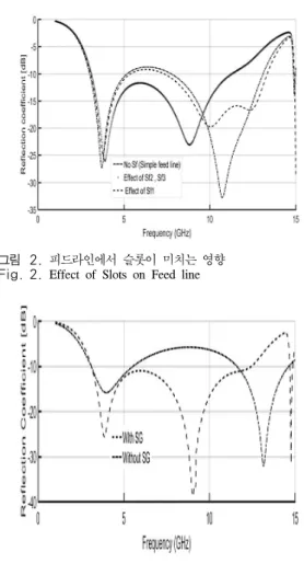
그림 2. 피드라인에서 슬롯이 미치는 영향 Fig. 2. Effect of Slots on Feed line
그림 3. 다른 접지에 대한 반사계수에 미치는 영향 Fig. 3. Effect on reflection coefficient with Different Ground
4 mm along with conventional (straight) microstrip feed line. The relation between rings is elaborated below
(6)
(7)
(8)
Whereas value of upper outer ring is same for both circle inside them such as
′ ′ (9)
In order to connect R1, R2 and R3 two rectangular slots named as and having same dimensions are used. Which provides the current path to the radiating patch and enhances the bandwidth, different dimensions parameters are used and analysed while simulation which concluded the optimized dimensions of 0.5 × 1.2 ㎜.
Bandwidth enhancement effect on proposed design because of slots on feed line which is termed as modified feed line and slotted ground (SG) are explained in section Ⅲ.
Ⅲ. Design and Analysis
Numerical simulations are carried out by a commercial available 3D full-wave electromagnetic field simulation tool (ANSYS HFSSv12).
3.1 Parametric Analysis
The simulated reflection coefficient for three parametric iterations is depicted together in Figure 2.
In other words this shows the effect of rectangular patch on feed line in terms of reflection coefficient.
Normally a conventional microstrip antenna does not show wide impedance bandwidth and it is clear from the simulated results as radiating patch significant mismatch with feed line over multiple frequency bands.
The impedance matching of the feed line with radiating patch is first enhanced by appropriate
adjustment of the width of the feed, getting an optimized value of 0.9 ㎜. The ground plane which plays important role in impedance matching network is optimized with adjust of two slots Sg1, Sg2
respectively. The reflection coefficient of this optimization is shown in Figure 3, it is apparent that the impedance bandwidth is improved at the middle end of the considered frequency band. As mentioned before the main purpose is to improve bandwidth while keeping overall size of the antenna minimum
3.2 Current Distribution Analysis
The current distribution normally gives an insight into the physical behavior of the antenna. Figure 4 shows the surface current distribution of the proposed small size antenna in term of vector representation at 3.8, 5.5, 7.5 and 5.5 ㎓
그림 6. 제안된 안테나의 시뮬레이션 반사계수
Fig. 6. Simulated Reflection coefficient [㏈] of the proposed antenna
(a) (b)
(c) (d)
그림 4. 다른 접지에 대한 반사계수에 미치는 영향 (a) 3.8
㎓m, (b) 5.5 ㎓, (c) 7.5 ㎓, (d) 10.2 ㎓
Fig. 4. Effect on reflection coefficient with Different Ground (a) 3.8 ㎓m, (b) 5.5 ㎓, (c) 7.5 ㎓, (d) 10.2 ㎓ respectively.
The surface current density mainly concentrates on the ground plane, radiator edges and feeding points. The current distribution at higher frequencies becomes more complex which is the indication of the higher order modes can be seen in Figure 4.
그림 5. 제안된 안테나의 시뮬레이션 VSWR
Fig. 5. Simulated Voltage standing wave ratio (VSWR) of the proposed antenna
Ⅳ. Simulation Result and Discussions
Figure 5 shows the simulated voltage standing wave ratio which can also be obtained by following equation.
(10)
When |Γ| = 0, optimal VSWR is obtained. This means that all power is transmitted to the antenna, and that there is no reflection. The impedance bandwidth of the proposed antenna is defined at VSWR≤2 so the proposed antenna satisfied for the bandwidth of 3.1 to 12.3 ㎓ with fractional Bandwidth of 122%.
10 ㏈ bandwidth of proposed design can be observed from Figure 6 with Bandwidth ratio of 4.13:1 and maximum return loss up to –38 ㏈.
A reasonable comparison between antennas, the authors[8] used an index term named as bandwidth dimension ratio (BDR) that allows antenna designers to guess the maximum bandwidth and degree of similarity compared to other existing designs. This index term indicates how
much operating bandwidth (in percentage) can be provided per unit electrical length.
×
(11)
Ref. Size [㎜] Footprint [㎟] BW
(S11≤10 ㏈) FBW (%) BDR BWR
[3] 49 × 55 2695 2.25 - 7.35 106.3 684 3.26:1
[4] 31 × 31 961 3.04 - 11 120 1248 3.62:1
[7] 25 × 25 625 3.5 - 9.25 90.2 1002 2.64:1
[8] 40 × 25 1000 0.9 - 22.35 184.5 20502 24.8:1
[9] 23.7 × 23.7 561.7 3.05 - 11.9 118 2049 3.9:1
[10] 28 × 29 812 5.73 - 10.8 61.3 301 1.88:1
This 15 × 12 180 3.1 - 12.8 122 6246 4.13:1
표 2. 면적, 대역폭 및 BDR 비교
Table 2. Dimensions, bandwidths and BDR comparison
그림 7. 주파수에 대한 그룹 지연 표현
Fig. 7. Group delay value representation against Frequency
(a) (b)
(c) (d)
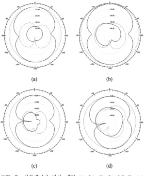
그림 8. 시뮬레이션 방사 패턴 (a) 3.1 ㎓ (b) 5.5 ㎓, (c) 7.5 ㎓, (d) 10.2 ㎓
Fig. 8. Simulated radiation pattern at (a) 3.1 ㎓, (b) 5.5
㎓, (c) 7.5 ㎓, (d) 10.2 ㎓ Where λ is the wavelength of the lower
frequency (initial) of the whole band meets the criteria of ≤ -10 ㏈. The comparison between proposed design and other antennas are summarized in Table 2. The antenna performance such as bandwidth, ratio bandwidth, Fractional bandwidth, footprints and BDR as listed as well.
Here, larger BDR value indicates that the design is smaller in dimensions and wider in bandwidth. It is noticeable that the relative permittivity of the substrate (which varies from material to material) is not considered in eq (2). In our case BDR value is 6246 which is better than many other design reported except in [8]. Main reason of difference between reference [8] and proposed design is antenna dimensions, as the size of this antenna is 2.5 times shorter than that reference paper. So it is concluded that dimension value difference is very obvious and can be clearly observed.
Group delay is very critical parameter in the antenna design because the shape of the transmitted
electrical pulse must not the distorted by the antenna while transmission. Indeed, for good pulse transmission and verification of the effectiveness of proposed antenna, the time domain response should be appropriate and the group delay must have very small and constant value throughout whole bandwidth. Figure 7 shows the simulated group delay of the proposed antenna for 3.1 to 12.3 ㎓. It is observed the group delay variation is less than 0.5 ns over the whole operating band except the value the 4 ㎓. Mostly if group delay variation is more than1ns it means the phases are no longer linear in
the far field region and chances of pulse distortion is more.
Figure 8 presents far field Radiation pattern of the proposed antenna in E-plane (Black Color) and H-plane (Gray Color) at 3.1, 5.5, 7.5 and 10.2 ㎓ respectively. It can be seen that proposed antenna shows omnidirectional behaviors on H-plane whereas, have the E-plane pattern have large black lobes and look like a doughnut or slightly pinched doughnut at lower frequency (3.1, 5.5), it starts to from humps , notches and becomes slightly smaller at higher frequencies (7.5, 10.2) ㎓.
Ⅴ. Conclusion
In this paper, a novel ultra-compact UWB antenna has been presented. The antenna is based on multiple circular rings with a modified feed line and slotted ground plane of dimensions 15 × 12 ㎜ having electrical dimensions of 0.14λ × 0.12λ (at lower initial frequency) and footprints of 180. This antenna has a good potential for wireless communication application i.e. WiMAX (3.3 ∼ 3.6
㎓), UWB (3.1 ∼ 10.6 ㎓), C-band (4 ∼ 8 ㎓), WLAN (5.15 ∼ 5.82 ㎓), X-band (7.9 ∼ 8.7 ㎓), MVDDS bands (12.2 ∼ 12.7 ㎓) because of its simple configuration, low profile and broad bandwidth. This design overtakes other state- of-the-art antenna structure reported in literature with respect to size and entire ultra wide bandwidth while maintaining acceptable performance level of electrical parameters. Bandwidth dimension ratio (BDR) factor, Bandwidth ratio (BWR) and fractional bandwidth (FBW) has been calculated in order to proof the novelty of the proposed design, which are in our case is 6246, 4.13:1 and 122% respectively.
References
[1] H. Schantz, The Art and Science of Ultra Wide-Band Antennas, Artech House, Norwood, MA, 2005.
[2] A. Rezaul, M. T Islam, and N. Misran,
“Compact tapered-shape slot antenna for UWB applications,” IEEE Ant. Wirel. Propag.
Lett., vol. 10, pp. 1190-1193, 2011.
[3] C. Deng, Y. J. Xie, and P. Li, “CPW-fed planar printed monopole antenna with impedance bandwidth enhanced,” IEEE Ant.
Wirel. Propag. Lett., vol. 8, pp. 1394-1397, 2009.
[4] M. Z. Mahmud, M. T. Islam, and M.
Samsuzzaman, “A high performance UWB antenna design for microwave imaging system,” Microw. and Optical Technol. Lett., vol. 58, no. 8, pp. 1824-1831, 2016.
[5] A. Bekasiewicz and S. Koziel, “Compact UWB monopole antenna for internet of things applications,” Electron. Lett., vol. 52, no. 7, pp. 492-49, 2016.
[6] M. N. Shakib, M. Moghavvemi, and W. N.
Mahadi, “A low-profile patch antenna for ultrawideband application,” IEEE Ant. Wirel.
Propag. Lett., vol. 14, pp. 1790-1793, 2015.
[7] M. S. Ellis, Z. Zhao, J. Wu, X. Ding, Z. Nie, and Q. H. Liu, “A novel simple and compact microstrip-fed circularly polarized wide slot antenna with wide axial ratio bandwidth for c-band applications,” IEEE Trans. Ant.
Propag., vol. 64, no. 4, pp. 1552-1555, 2016.
[8] F. A. Tahir and A. H. Naqvi, “A compact hut-shaped printed antenna for super wideband applications,” Microw. Optical Technol. Lett., vol. 57, no. 11, pp. 2645-2649, 2015.
[9] B. Gong, X. S. Ren, Y. Y. Zeng, L. H. Su, and Q. R. Zheng, “Compact slot antenna for ultra-wide band applications,” IET Microw., Ant. Propag., vol. 8, no. 3, pp. 200-205, 2014.
[10] N. George and B. Lethakumary, “A compact microstrip antenna for UWB applications,”
Microw. Optical Technol. Lett., vol. 57, no.3, pp. 621-624, 2015.
[11] D. Y. Choi, S. W. Kim, J. J. Park, M. A Jeong, and S. R. Lee, “Design and implementation of tapered slot antenna for ship's indoor location-aware system,” J. KICS, vol. 39C, no. 12, pp. 1307-1313, Dec. 2014.
[12] J. J. Kim, S. W. Kim, J. J. Park, M. A Jeong, K. W. Park, and D. Y. Choi, “Design and analysis of UWB circular patch antenna using
microstrip line,” J. KICS, vol. 40, no. 05, pp.
938-943, May 2015.
[13] K. J. Jeon, B. H. Ko, S. C. Myung, S. R. Lee, and K. S. Kim, “Protograph-based block LDPC code design for marine satellite communications,” J. KICS, vol. 39C, no. 7, pp. 515-520, Jul. 2014.
[14] S. W. Kim and D. Y. Choi, “Compact filtering monopole patch antenna with dual‑.band rejection,” SpringerPlus, vol. 5, no. 1, pp. 1-12, 2016.
[15] S. W. Kim and D. Y. Choi, “Implementation of rectangular slit‑inserted ultra‑wideband tapered slot antenna” SpringerPlus, vol. 5, no.
1, 2016.
이람 나담 (Iram Nadeem)
2016년 3월~현재:조선대학교 정보통신공학과 석사과정
<관심분야> UWB 안테나, 소 형 안테나 설계
김 영 진 (Young-Jin Kim)
1988년 8월:조선대학교 전자 공학과 석사
2003년 2월:조선대학교 전자 공학과 박사
<관심분야> IR-UWB 레이더, 안테나 설계, 네트워크
![Table 1. Optimized dimensions in (㎜) of proposed antennadimensions of antenna[8]](https://thumb-ap.123doks.com/thumbv2/123dokinfo/5272016.370095/3.799.94.366.84.678/table-optimized-dimensions-proposed-antennadimensions-antenna.webp)