선결정화법을 이용한 금속 유도 일측면 결정화에 의해 제작된 다결정 실리콘 박막 트랜지스터 소자 및 회로의
전기적 특성 개선 효과
황욱중a,b,c, 강일석a*, 김영수c, 양준모a,c, 안치원a,c, 홍순구b
a나노종합팹센터 정보전자부품소재기술혁신센터, 대전 305-806
b충남대학교 재료공학과, 대전 305-764
c나노종합팹센터, 대전 305-806
(2008년 8월 1일 받음, 2008년 9월 23일 수정, 2008년 9월 25일 확정)
적층 박막 내에서의 상변화는 주변 층에 영향을 준다. 결정화가 게이트 절연층에 주는 영향이 제거된 선결정화법 (precrystallization)이 금속 유도 일측면 결정화(metal-induced unilateral crystallization)에 의해 제작된 다결정 실리콘 박막 트랜지스터 소자 및 회로의 전기적 특성에 미치는 영향에 대하여 연구하였다. 이 방법으로 만들어진 소자는 일반적인 후 결정화(postcrystallization) 소자에 비하여 높은 전류 구동력을 보였다. 여기에 본 연구는 DC bias에 의한 ring oscillator의 특성 변화를 연구하였다. 선결정화된 실리콘 박막을 이용하여 제작한 PMOS inverter는 후결정화된 실리콘 박막을 이용하여 제작한 inverter에 비하여 매우 동적(dynamic)이고도 안정적인 특성을 보였다.
주제어 : 금속 유도 일측면 결정화, 다결정 실리콘 박막 트랜지스터, 선결정화법, ring oscillator
Ⅰ. 서 론
최근 system-on-glass(SOG) 구현을 위하여 수소화 비정 질 실리콘(a-Si:H)에 비해 전계 효과 이동도(field-effect mobility)와 박막 트랜지스터(thin-film transistor, TFT)의 구동 안정성이 뛰어난 저온 다결정 실리콘(low-temperature polycrystalline silicon, LTPS)에 대한 관심이 커지고 있다.
유리 기판 위에 대면적으로 다결정 실리콘을 만드는 여러 방법[1-2] 중 금속 유도 일측면 결정화법(metal-induced unilateral crystallization, MIUC)은 가능성 높은 한 방법 이다[3]. MIUC란 금속과 실리콘이 반응하여 형성된 금속 실리사이드가 촉매로써 결정화 온도를 낮추고 한쪽 측면으 로부터 이동하면서 결정화가 진행되는 현상으로, 기존 양 측 결정화가 지닌 단점, 즉 양쪽에서부터 결정화가 진행되 어온 경계(crystal growth joint) 결함을 채널 밖으로 제거 하는 기술이다.
현재까지 알려진 MIUC 메커니즘 모델은 미시적으로 측 면 결정화가 이루어지는 동안 결합의 파괴와 생성, 인장
(tensile)과 압축(compressive) 변형(strain)이 반복해서 일어남을 보여 준다[4]. 이러한 일련의 변화들은 게이트 형 성 후 측면 결정화와 도펀트 활성화(dopant activation)를 동시에 하는(후결정화, postcrystallization) 일반적인 TFT(이하 post-TFT)의 게이트 절연층 또는 게이트 절연 층과 실리콘 활성층(active layer) 사이의 계면에 영향을 줄 것이다.
본 연구에서는, 게이트 절연층이 측면 결정화의 영향을 받지 않도록 측면 결정화한 후 게이트를 형성한(선결정화, precrystallization) p-type TFT(이하 pre-TFT)를 제작 하였다. 선결정화가 MIUC poly-Si TFT의 전기적 특성에 미치는 영향을 관찰하였고, ring oscillator를 제작함으로 써 선결정화로 제작된 소자가 주변 회로용으로 쓰이기에 적합함을 증명하였다.
Ⅱ. 실험방법
황욱중 ․ 강일석 ․ 김영수 ․ 양준모 ․ 안치원 ․ 홍순구
Fig. 1. Comparison of fabrication process flow between
pre
-TFT andpost
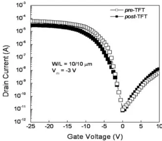
-TFT.Fig. 3. Comparison of typical transfer characteristics between
pre
-TFT andpost
-TFT.Fig. 2. The line data from AFM of the sample in process of lateral crystallization.
pre-TFT와 post-TFT의 제작 공정 순서를 비교하여 Fig. 1에 나타내었다. pre-TFT의 자세한 제작 방법은 다 음과 같다. 유리 기판 위에 플라즈마 화학기상증착 (plasma-enhanced chemical vapor deposition, PECVD)으로 완충층 3000 Å 두께의 실리콘 산화막(SiO2) 을 증착하였다. Si2H6 가스(disilane)를 사용하는 저압 화 학기상증착(low-pressure CVD, LPCVD)으로 600 Å 두 께의 비정질 실리콘을 증착하였다. 반응성 이온식각 (reactive ion etching, RIE)으로 실리콘 활성층을 패터닝 한 후 MIUC의 촉매 금속인 100 Å 두께의 니켈 창 (window)을 lift-off 공정으로 형성하였다. 580 ℃ 수소 분위기에서 세 시간 동안 결정화를 진행하였다. 게이트 절 연층으로 700 Å 두께의 SiO2를, 게이트 금속의 접착력을 높이기 위하여 200 Å 두께의 Ti를, 그리고 게이트 금속 층으로 2000 Å 두께의 TiW을 각각 PECVD와 스퍼터링으 로 증착하였다. 그리고 TiW, Ti, SiO2 세 층을 각각 RIE로 패터닝 하였다. 소오스와 드레인을 형성하기 위하여 B2H6
를 도핑하였다(ion mass doping, IMD). 가속 전압과 RF 파워는 각각 15 kV와 150 W이었다. 급속 열처리(rapid thermal annealing, RTA)를 이용한 도펀트 활성화 (dopant activation)를 580 ℃에서 한 시간 동안 진행하였 다. 이후 contact window와 소오스/드레인 금속 라인 형 성은 일반적인 TFT 제작 과정과 동일하게 진행하였다. 비 교를 위하여 게이트 형성 후 측면 결정화와 도펀트 활성화 를 동시에 진행한 post-TFT도 제작하였다. keithley 4200 semiconductor characterization system을 사용하여 전 류-전압(I-V)곡선 그래프를 얻었다.
Ⅲ. 실험결과 및 고찰
Fig. 2는 비정질 실리콘의 양쪽 측면으로부터 결정화되는 과정에서 얻은 원자력 현미경(atomic force microscope, AFM)의 라인 데이터이다[5]. 결정 과정에서 평균 1.65 ± 0.15 %의 두께 수축이 일어났음을 알 수 있다. 이러한 두께 변화는 pre-TFT 보다 post-TFT의 박막 내에서 더 심한 압축 응력을 야기할 것이다[6]. 왜냐하면 후결정화되는 동 안에 Si/SiO2 계면에 쌓일 것으로 예상되는 응력이 선결정 화되는 동안에는 위로 풀리는 것이기 때문이다. PMOSFET 에 가한 압축 응력이 정공(hole)의 이동도를 향상시킨다는 보고[7]와는 달리, 본 실험의 결과에서는 p-type post-TFT에서 이동도 감소가 나타났다. 결국 결합의 파괴 와 생성을 비롯한, 측면 결정화로 야기되는 응력의 고유한 요인들(unique factors)이 Si/SiO2 계면의 질(quality)을 손상시키는 것으로 보인다.
Fig. 4. Schematic circuit of PMOS ring oscillator consisted of 5-stage inverters.
Fig. 5. Dependence of propagation delay time on supply voltage of 5-stage PMOS ring oscillators fabricated using precrystallization and postcrystallization.
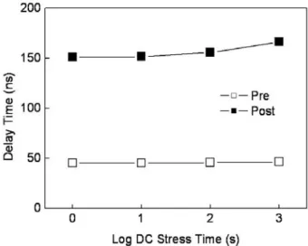
Fig. 6. DC bias-stress (at VDD = -20 V) effect on delay time for
pre
-TFT andpost
-TFT ring oscillators.우리의 이전 보고에서는 이와 같은 소자 특성 차이의 근 본 이유로 측면 결정화되는 동안 Si/SiO2 계면에서 생성된 interface state를 제시하였다[8]. 즉, 전하를 띄는 interface state에 의한 Coulomb 산란이 이동도를 떨어뜨 리게 되는 것이다. 본 연구에서 ring oscillator 제조에 사 용한 pre-TFT와 post-TFT의 특성을 Fig. 3에 비교하였 다. 이전 보고와 같이, pre-TFT의 이동도는 58 cm2/Vs로, post-TFT의 30 cm2/Vs에 비하여 높았다.
Fig. 4는 5단(stage)의 inverter로 구성된 PMOS ring oscillator의 회로도이다. Fig. 5는 공급 전압(supply voltage, VDD)에 대한 ring oscillator의 전파 지연 시간 (propagation delay time) 변화를 나타내었다. 평균 전파 지연 시간을 1/(2Nfosc)로 정의할 때, pre-TFT로 구성된 회로의 전파 지연 시간은 -20 V에서 45.3 ns로 나왔으며, 이는 post-TFT로 구성된 회로보다 약 1/2 자릿수(order
of magnitude)만큼 더 작은 수치였다. 이때 fosc는 출력 파 형(output waveform)에서의 ring oscillator 진동수이며, N은 inverter 체인의 개수이다[9].
VDD가 -20 V일 때, DC bias-stress 시간에 따른 pre-TFT와 post-TFT ring oscillator의 열화 정도를 Fig.
6에 비교하였다. 실험 결과에 의하면 pre-TFT ring oscillator의 지연 시간에는 변화가 적었다. 반면에 post-TFT ring oscillator는 1000초가 지난 후 눈에 띄게 열화 되었다. 이는, poly-Si TFT에 대한 bias-stress 효 과가 게이트 절연막질에 크게 의존한다는 선행 연구의 결 과로 설명될 수 있다[10].
Ⅳ. 결 론
선결정화법을 사용하여 부피 수축으로 발생되는 응력을 MIUC poly-Si TFT로부터 추출해 내었고, 이것이 소자와 회로의 전기적 특성에 미치는 영향을 연구하였다. 후결정 화와 비교하여 캐리어 이동도가 두 배 가까이 더 높았다.
더욱이 pre-TFT ring oscillator는 post-TFT ring oscillator에 비하여 매우 동적(dynamic)이고도 안정적인 특성을 보였다. 따라서 본 연구에서 제안한 방법은 진보된 TFT 회로 제작 기술의 하나로 미래 전자 시스템 분야에 적 용될 수 있을 것이다.
황욱중 ․ 강일석 ․ 김영수 ․ 양준모 ․ 안치원 ․ 홍순구
감사의 글
본 연구는 지식경제부 지역전략산업진흥사업의 지역혁 신기반구축사업(과제번호:B0010341)의 지원으로 수행되 었습니다.
참고문헌
[1] R. B. Iverson and R. Reif, J. Appl. Phys. 62, 1675 (1987).
[2] K. H. Kim, S. J. Park, K. S. Cho, W. S. Sohn, and J. Jang, SID Tech. Dig., 150 (2002).
[3] Z. Meng, M. Wang,and M. Wong, IEEE Trans.
Electron Devices 47, 404 (2000).
[4] N. -K. Song, M. -S. Kim, S. -H. Han, Y. -S. Kim, and S. -K. Joo, J. Electrochem. Soc. 154, H370 (2007).
[5] T. H. Kim, H. I. Kwon, J. D. Lee, and B. G. Park, Int. Microprocesses and Nanotechnology Conf.
2001, 240 (2001).
[6] T. P. Leevard Pedersen, J. Kalb, W. K. Njoroge, D. Wamwangi, M. Wuttig, and F. Spaepen, Appl.
Phys. Lett. 79, 3597 (2001).
[7] A. Oishi, O. Fujii, T. Yokoyama, K. Ota, T. Sanuki, H. Inokuma, K. Eda, T. Idaka, H. Miyajima, S.
Iwasa, H. Yamasaki, K. Oouchi, K. Matsuo, H.
Nagano, T. Komoda, Y. Okayama, T. Matsumoto, K. Fukasaku, T. Shimizu, K. Miyano, T. Suzuki, K. Yahashi, A. Horiuchi, Y. Takegawa, K. Saki, S. Mori, K. Ohno, I. Mizushima, M. Saito, M. Iwai, S. Yamada, N. Nagashima, and F. Matsuoka, IEDM Tech. Digest, 239 (2005).
[8] I. -S. Kang, S. -H. Han, and S. -K. Joo, Appl. Phys.
Lett. 91, 092112 (2007).
[9] S. Docking and M. Sachdev, IEEE J. Solid-State Circ. 39, 533 (2004).
[10] J. H. Lee, M. Y. Shin, K. C. Moon, and M. K.
Han, Phys. Scripta. T114, 199 (2004).
Dynamic Characteristics of Metal-induced Unilaterally Crystallized Polycrystalline Silicon Thin-film Transistor Devices and Circuits Fabricated
with Precrystallization
Wook-Jung Hwanga,b,c, Il-Suk Kanga*, Young-Su Kimc, Jun-Mo Yanga,c, Chi-Won Ahna,c, and Soon-Ku Hongb
a
Advanced Technology Center for Information Electronic Materials and Components, National Nanofab Center, Daejoen 305-806
b
Department of Materials Science and Engineering, Chungnam National University, Daejoen 305-764
c
National Nanofab Center, Daejoen 305-806
(Received August 1, 2008, Revised September 23, 2008, Accepted September 25, 2008)
The phase transformation in a film influences its surrounding. Effects of the precrystallization method, which removes influences on gate oxide caused by lateral crystallization, in metal-induced unilaterally crystallized polycrystalline silicon thin-film transistor devices and circuits were studied. Device by the method was shown to have a higher current drive, compared with conventional postcrystallized device. Moreover, we studied DC bias-induced changes in the performance of ring oscillator. PMOS inverters fabricated using precrystallized silicon films have very high dynamic and stable performance, compared with inverters fabricated using postcrystallized silicon films.
Keywords : Metal-induced unilateral crystallization, Polycrystalline silicon thin-film transistor, Precrystallization, ring oscillator
* [E-mail] [email protected]