Vol. 27, No. 2 (2017) 75-79
https://doi.org/10.6111/JKCGCT.2017.27.2.075
e-ISSN 2234-5078
Comparison of characteristics of silver-grid transparent conductive electrodes for display devices according to fabrication method
Byoung Su Choi, Seok Hwan Choi*, Jeong Ho Ryu** and Hyun Cho*
,†Department of Nano Fusion Technology, Pusan National University, Miryang 50463, Korea
*Department of Nanomechatronics Engineering, Pusan National University, Busan 46241, Korea
**Department of Materials Science and Engineering, Korea National University of Transportation, Chungju 27469, Korea (Received April 13, 2017)
(Revised April 18, 2017) (Accepted April 19, 2017)
Abstract Honeycomb-shaped Ag-grid transparent conductive electrodes (TCEs) were fabricated using two different processes, high density plasma etching and lift-off, and the optical and electrical properties were compared according to the fabrication method. For the fabrication of the Ag-grid TCEs by plasma etching, etch characteristics of the Ag thin film in 10CF
4/5Ar inductively coupled plasma (ICP) discharges were studied. The Ag etch rate increased as the power increased at relatively low ICP source power or rf chuck power conditions, and then decreased at higher powers due to either decrease in Ar
+ion energy or Ar
+ion-assisted removal of the reactive F radicals. The Ag-grid TCEs fabricated by the 10CF
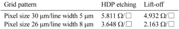
4/5Ar ICP etching process showed better grid pattern transfer efficiency without any distortion or breakage in the grid pattern and higher optical transmittance values of average 83.3 % (pixel size 30 μm/line width 5 μm) and 71 % (pixel size 26 μm/line width 8 μm) in the visible range of spectrum, respectively. On the other hand, the Ag-grid TCEs fabricated by the lift-off process showed lower sheet resistance values of 2.163 Ω/□ (pixel size 26 μm/line width 8 μm) and 4.932 Ω/□ (pixel size 30 μm/line width 5 μm), respectively.
Key words Ag-grid transparent conductive electrodes, High density plasma etching, Lift-off, Optical transmittance, Sheet resistance
제조공법에 따른 디스플레이 소자용 silver-grid 투명전극층의 특성 비교
최병수, 최석환*, 류정호**, 조현*
,†부산대학교 나노융합기술학과, 밀양, 50463
* 부산대학교 나노메카트로닉스공학과, 부산, 46241
**한국교통대학교 신소재공학과, 충주, 27469 (2017년 4월 13일 접수)
(2017 년 4월 18일 심사완료) (2017 년 4월 19일 게재확정)
요 약 고밀도 플라즈마 식각 및 lift-off 두 가지 공정으로 honeycomb 형상의 Ag-grid 투명전극층을 제작하였고 제조 공법에 따른 광학적 및 전기적 특성을 비교하였다. 플라즈마 식각 조건 선정을 위하여 Ag 박막의 10CF
4/5Ar 유도결합 플 라즈마 식각특성을 조사하였다. 비교적 낮은 ICP source power 또는 rf chuck power 영역에서는 power 증가에 따라 Ag 식 각속도가 증가하였고, 높은 power 조건에서는 Ar
+이온 에너지 감소 또는 Ar
+이온에 의한 F radical 제거로 인해 식각속도 가 감소하였다. 10CF
4/5Ar 플라즈마 식각 공정에 의해 제작된 Ag-grid 전극층은 lift-off 공정으로 제작된 전극층에 비해 grid 패턴 형상의 왜곡이나 단절이 없는 더 우수한 grid 패턴 전사 효율과 가시광선 영역에서 더 높은 83.3 %(pixel 크기 30 μm/선폭 5 μm)와 71 %(pixel 크기 26 μm/선폭 8 μm)의 광투과율을 각각 나타내었다. 반면에 lift-off 공정으로 제작된 Ag- grid 전극층은 플라즈마 식각 공정 시편보다 더 우수한 2.163 Ω/□(pixel 크기 26 μm/선폭 8 μm)과 4.932 Ω/□(pixel 크기 30 μm/선폭 5 μm)의 면저항 특성을 나타내었다.
†
Corresponding author
†
E-mail: [email protected]
격하게 증가하였다[1-5]. 투명전도성 전극은 다양한 소자 의 핵심 구성요소로서 응용분야에 따라 다소 차이가 있 지만 가시광선 영역에서 평균 80 % 이상의 높은 광투과 율과 약 15 Ω/□ 이하의 면저항 특성이 요구된다.
위에 기술한 다양한 응용분야에서 현재 가장 널리 사 용되고 있는 투명전도성 전극재료는 indium tin oxide (ITO) 이다. 물리적 기상증착법인 sputtering 공정에 의해 주로 제조되는 ITO는 400~700 nm 파장대의 가시광선 영역에서 평균 약 87 % 정도의 높은 광투과율과 우수한 면저항 특성을 나타내는 것으로 알려져 있다. 그러나 ITO 투명전도성 전극은 몇 가지 한계에 직면해 있다. 우 선 주 구성원소인 indium의 희소성으로 인해 높은 제조 비용을 부담해야 하는 문제가 있다. ITO 기반 터치스크 린의 경우 제조비용 중 약 25 %에 가까운 비용을 ITO 전극층 형성에 투입하는 것으로 파악되며 관련 기업들은 제조원가 절감을 위해 노력하고 있다. 또한 상대적으로 높은 저항문제로 인해 대면적화가 용이하지 않고, ITO 특유의 취성으로 인해 유기 발광 다이오드(organic light emitting diodes, OLEDs) 를 기반으로 하는 유연성 디스 플레이(flexible display)에 적용하기가 어려운 취약점을 가진다[6-8].
따라서 기존 ITO의 단점을 극복하기 위하여 가시광선 영역에서의 높은 광투과율, 낮은 면저항 뿐만 아니라 제조 비용이 저렴하고 유연성을 가지는 새로운 TCE를 개발하 기 위하여 최근에 많은 연구가 진행되고 있다. 현재까지 Poly(3,4-ethylenedioxythiophene) : polystyrene sulfonate (PEDOT : PSS) 와 같은 전도성 폴리머, 나노미터 스케일 의 금속 박막, 금속 grid, 탄소 나노튜브, 그래핀 등이 ITO 를 대체할 새로운 TCE 소재로 제안되었다[9-11]. 이 들 중에서 Cu, Al, Ag 등의 전도성 금속 grid 기반 TCE 는 제조비용이 저렴하고 기계적 특성이 우수한 동시 에 grid 선폭과 간격, 두께 변화를 통해 광투과율과 면 저항을 정밀하게 제어하는 것이 가능하여 ITO를 대체할 새로운 TCE로 인식되고 있다[12-15].
본 연구에서는 투명한 고분자재료인 polyethylene ter- ephtalate(PET) 기판에 우수한 면저항과 내산화 특성을 가지는 silver(Ag)의 grid 구조를 고밀도 플라즈마 식각 (high density plasma etching) 및 lift-off의 두 가지 방 법으로 제작하였고 제조공법 및 grid 패턴 형상에 따른 광학적 특성과 전기적 특성을 비교하였다.
500 nm 두께의 Ag/Si 박막을 3 × 10
−4Torr 압력 조건에서 E-beam evaporation 법으로 증착하고, AZ 5214 photoresist (PR) 로 패터닝한 후 planar type 유도결합 플라즈마 (inductively coupled plasma, ICP) 식각장치를 이용하여 식각하였다. 식각 공정 가스로는 Ag와의 반응성을 고려 하여 10CF
4/5Ar( 총 유량 15 sccm) 혼합가스를 사용하였 다. ICP source power와 rf chuck power는 각각 100~
400 W, 100~250 W 범위로 변화시켰고, 공정압력은 10 mTorr 로 유지하였다. 식각 후 stylus profilometry 장비 를 이용하여 식각속도를 분석하였다.
플라즈마 식각에 의한 Ag-grid 제작은 Ag 층 증착, photolithography 패터닝, 플라즈마 식각의 순서로 진행 하였다. 먼저 PET 기판 위에 두께 약 100 nm의 Ag 층을 E-beam evaporation 법으로 증착한 후 photolithography 공정으로 AZ 5214 PR 층에 두 가지 형상의 honeycomb 패턴(pixel 크기 30 μm/선폭 5 μm 및 pixel 크기 26 μm/
선폭 8 μm)을 전사하였다. 식각속도 분석을 통해 선정한 조건(ICP source power 200 W, rf chuck power 100 W) 을 적용하여 Ag 층을 식각한 후 표면 세척하여 Ag-grid 제작을 완료하였다.
두 번째 방법인 lift-off 공정에 의한 Ag-grid 제작은 PET 기판상에 AZ 5214 PR층을 spin coating으로 도포 하고 photolithography 공정으로 위와 동일한 두 가지 honeycomb 패턴을 전사하였다. 이후 두께 약 100 nm의 Ag 층을 E-beam evaporation법으로 증착한 후 아세톤 수조에서 lift-off 및 DI water 초음파 세척을 진행하여 Ag-grid 를 제작하였다.
두 가지 공법으로 제작된 Ag-grid 전극층의 구조적 특 성, 광투과율 및 면저항은 광학현미경, UV-VIS spectro- photometer, 4-point probe 장비를 이용하여 비교분석하 였다.
3. 결과 및 고찰
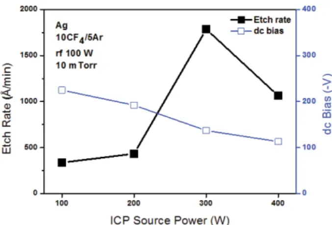
Fig. 1 은 10CF
4/5Ar 유도결합 플라즈마에서 ICP source power 증가가 Ag 식각속도에 미치는 영향을 보여주고 있다. ICP power가 300 W까지 증가함에 따라 Ag 식각 속도가 계속적으로 증가하고 300 W 조건에서 가장 높은
~1790 Å/min의 식각속도를 나타낸 후 식각속도가 감소
하였다. 10CF
4/5Ar 혼합가스에 인가하는 ICP power 증 가는 혼합가스의 해리반응을 활성화시키게 되므로 플라 즈마 내에 존재하는 fluorine(F) radical 밀도를 증가시키 게 된다. 증가된 F radical들은 Ag 표면 원자들과의 화 학적 반응을 통해 플루오르화 은(Ag
xF
y) 식각 반응물을 생성하게 되고 식각 반응물 생성량은 F radical 밀도에 비례하여 증가하게 된다, 표면에 형성된 식각 반응물에 Ar
+이온포격에 의한 에너지가 적절한 수준으로 전달되 면 생성된 식각 반응물들이 표면으로부터 제거되는 과정 을 통해 식각속도가 증가하게 될 것이다[16]. ICP 100~
300 W 구간에서는 식각 반응물 생성과 식각 반응물 제 거 간에 균형이 유지되어 식각속도가 계속적으로 증가한 반면에 400 W 조건에서는 표면에 다량으로 생성된 식각 반응물들을 효율적으로 제거하기에 충분한 Ar
+이온 에 너지가 공급되지 않음에 따라 식각속도가 감소한 것으로 사료된다.
Rf chuck power 증가가 Ag 식각속도에 미치는 영향 을 Fig. 2에 제시하였다. 플라즈마 식각의 효율성을 지 배하는 화학적 요소와 물리적 요소 중 물리적 요소는 이
온포격에 참여하는 Ar
+이온들의 평균에너지에 의해 결 정된다. Ar
+이온들이 시편표면에 충돌할 때 전달되는 평균에너지는 인가해준 rf chuck power에 비례하며 증 가하게 된다. Rf chuck power 100~200 W 구간에서는 rf chuck power 증가에 따라 Ar
+이온들의 이온포격에 의한 Ag
xF
y식각 반응물의 제거가 증진됨에 따라 Ag 식각속도가 향상됨을 알 수 있다. 그러나 rf chuck power 250 W 조건에서는 식각속도가 감소하였는데, 이는 F radical 들이 시편 표면에서 Ag 표면원자와의 화학적 반 응을 통해 Ag
xF
y식각 반응물을 형성하기 전에 고에너 지 상태의 Ar
+이온들에 의해 제거되기 때문인 것으로 생각된다.
Fig. 3 은 플라즈마 식각 공정에 의해 제조된 두 가지 패턴 형상(pixel 크기 30 μm/선폭 5 μm 및 pixel 크기 26 μm/선폭 8 μm)의 Ag-grid를 광학현미경으로 관찰한 이미지이다. Ag 층의 플라즈마 식각은 PR burning out, ion damage 에 의한 전기적 특성 저하 및 PET 기판 변 형 등을 최소화하기 위하여 Fig. 1과 Fig. 2에서 조사한 식각 조건들 중에서 ICP power 200 W, rf chuck power 100 W 낮은 인가 power 조건을 적용하였다. 그림에서 보는 바와 같이 플라즈마 식각 공정에 의해 제조된 Ag- grid 는 형상의 왜곡이나 균열 발생이 없이 pixel 형태 및 선폭이 균일하게 구현된 구조적 특성을 나타냄을 알 수 있었다.
Lift-off 공정에 의해 제조된 두 가지 패턴(pixel 크기
Fig. 2. Ag etch rate as a function of rf chuck power in 10CF
4/ 5Ar ICP discharges (200 W source power, 10 mTorr).
Fig. 4. Optical micrographs of Ag-grid electrodes fabricated by lift-off process.
Fig. 3. Optical micrographs of Ag-grid electrodes fabricated by 10CF
4/5Ar inductively coupled plasma etching process.
Fig. 1. Ag etch rate as a function of ICP source power in
10CF
4/5Ar ICP discharges (100 W rf chuck power, 10 mTorr).
이 관찰되었다. 이러한 현상은 증착된 Ag 층과 PET 기 판 사이의 낮은 밀착성(adhesion), AZ 5214 PR 층과 PET 기판 간의 낮은 밀착성을 포함한 photolithography 공정의 효율성 저하 등으로 인해 발생했을 가능성이 높 은 것으로 판단되며 정확한 원인 규명을 위해서는 추가 적인 연구가 필요한 것으로 사료된다.
Fig. 5 는 플라즈마 식각 공정으로 제작된 Ag-grid 시 편의 광투과율을 380~700 nm의 가시광선 영역에서 UV- VIS spectrophotometer 로 측정한 스펙트럼이다. 그림에 서 보는 바와 같이 두 가지 패턴의 Ag-grid 시편 모두 특정 파장대에서의 흡수대는 관찰되지 않았고, 가시광선
영역에서 pixel 크기 30 μm/선폭 5 μm Ag-grid 시편은 평균 83.3 %, pixel 크기 26 μm/선폭 8 μm의 Ag-grid는 이보다 낮은 평균 71 %의 광투과율을 각각 나타내었다.
이러한 차이는 Ag-grid pattern 선폭이 증가함에 따라 입사광을 투과시킬 수 있는 개방 면적(open area)이 감 소하기 때문에 발생한 것으로 이해된다.
동일한 파장 영역에서 측정한 lift-off 공정으로 제작된 Ag-grid 시편의 광투과율을 Fig. 6에 제시하였다. Pixel 크기 30 μm/선폭 5 μm Ag-grid 시편은 평균 80 %, pixel 크기 26 μm/선폭 8 μm Ag-grid는 평균 60.1 %의 광투 과율을 각각 나타내었다. Lift-off 공정으로 제작된 Ag- grid 시편들이 플라즈마 식각 공정으로 제작된 Ag-grid 시편들에 비해 낮은 광투과율 특성을 나타내었는데 이는 lift-off 과정에서 PET 기판 상에서 완전히 제거되지 않 은 PR 또는 Ag 층의 잔류물(residue)에 의한 광투과율 저하 때문인 것으로 판단된다.
플라즈마 식각 공정, lift-off 공정의 두 가지 공법으로 제작된 Ag-grid 시편들의 면저항을 4-point probe로 측 정한 결과를 Table 1에 정리하였다. 제시된 면저항 수치 는 제조공법 및 grid pattern별로 각각 5개씩 제작된 시 편으로부터 측정된 결과의 평균치이며, lift-off의 경우 불완전한 pixel 패턴 전사 및 grid 형태 단절이 관찰된 시편은 측정 대상에서 제외하였다. 앞서 제시한 광투과 율 측정결과와 대조적으로 Ag-grid 선폭이 증가함에 따 라 면저항이 감소하였는데 이는 선폭 증가에 따라 Ag- grid 의 단면적이 증가하였기 때문으로 광투과율과 면저 항 간 trade-off가 존재함을 확인하였다. 또한 동일한 grid 패턴에 대해 플라즈마 식각공정으로 제작된 Ag-grid 전 극층이 lift-off Ag-grid 전극층에 비해 조금 높은 면저항 을 나타내었는데, 이는 플라즈마 식각 과정에서 발생한 ion charging 효과와 다소간의 연관성이 있을 것으로 생 각된다[18].
4. 결 론
플라즈마 식각 및 lift-off 두 가지 공정으로 Ag-grid 투명 전극층을 제작하였고 제조공법에 따른 광학적 및 전기적 특성 차이를 조사하였다. 플라즈마 식각 공정 조 건 선정을 위하여 Ag 박막의 10CF
4/5Ar 유도결합 플라 Fig. 5. Optical transmittance spectra of Ag-grid electrodes fab-
ricated by 10CF
4/5Ar inductively coupled plasma etching process.
Fig. 6. Optical transmittance spectra of Ag-grid electrodes
fabricated by lift-off process.
즈마 식각특성 조사를 먼저 진행하였고, ICP power 및 rf chuck power 가 Ag 식각 속도에 미치는 영향을 분석 하였다. 플라즈마 식각 공정에 의해 제작된 Ag-grid 전 극층은 형상의 왜곡이나 균열 발생이 없이 pixel 형태 및 선폭이 균일하게 구현된 반면에 lift-off 공정으로 제 작된 일부 시편에서는 Ag 층과 PET 기판 사이의 밀착 성 문제 또는 photolithography 공정 효율성 저하로 인 해 불완전한 pixel 패턴 전사 및 grid 형태 단절이 관찰 되었다. 플라즈마 식각 공정으로 제작된 pixel 크기 30 μm/선폭 5 μm 및 pixel 크기 26 μm/선폭 8 μm의 Ag- grid 전극층은 lift-off 공정보다 더 높은 평균 83.3 % 및 71 % 의 광투과율을 가시광선 영역에서 각각 나타내었다.
이와 대조적으로 면저항 특성은 선폭이 증가함에 따라 향상되었고, lift-off 공정으로 제작된 Ag-grid 전극층이 더 좋은 면저항 특성을 나타내었다.
References