• 검색 결과가 없습니다.

A Voltage-Lift DC-DC Converter with Large Conversion Ratio

N/A
N/A
Protected

Academic year: 2021

Share "A Voltage-Lift DC-DC Converter with Large Conversion Ratio"

Copied!
7
0
0

로드 중.... (전체 텍스트 보기)

전체 글

(1)

A Voltage-Lift DC-DC Converter with Large Conversion Ratio

Ho-Yeon Kim

*

, Eun-A Moon

**

, Yong-Mi Lee

*

, Youn-ok Choi

***

Abstract

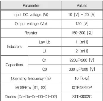
A extension of the high boost voltage-lift DC-DC converter with large conversion ratio has been proposed in this paper. The proposed extension is combined the switched-inductor cell (SL-cell) and modular voltage cell (MV-cell). The proposed structure can achieve the large voltage conversion without high duty-cycle and the low voltage of the components. Moreover, the PID controller for novel SL-MV voltage-lift DC-DC converter also introduces. This technique a good-performance output voltage can kept constant with an good transient performance when the output load is suddenly changed. In order to prove the theoretical analysis, the experimental setup has been built for the DC load of 150[Ω] and 300[Ω]. In addition, the transient of output voltage has been tested to determine the controller. Experimental results validate the effectiveness of the theoretical analysis proving the satisfactory converter performance.

Key words:tranformerless converter; high-voltage gain; switched-inductor; voltage-lift; duty ratio

* Dept. of Electrical Engineering, College of Korea Polytechnies

** Dept. of Electrical Engineering, Chosun College of Science & Technology

*** Dept. of Electrical Engineering, Chosun University

★ Corresponding author

E-mail:[email protected], Tel:+82-62-230-7175

※ Acknowledgment

This study was supported by research fund from Chosun University, 2017 Manuscript received Sep. 2, 2019; revised Oct. 25, 2019; accepted Nov. 15, 2019.

This is an Open-Access article distributed under the terms of the Creative Commons Attribution Non-Commercial License (http://creativecommons.org/licenses/by-nc/3.0) which permits unrestricted non-commercial use, distribution, and reproduction in any medium, provided the original work is properly cited.

Ⅰ. Introduction

Nowadays, energy from renewable sources such as wind power, photovoltaic power, and fuel cells has become the best solution to generate clean electric energy. However, the demerit characteristics of these energies is the low-output voltage and instability. Thus, a DC-DC converters [1-2] with a high boost voltage conversion is used to boost the low output voltage of the clean energy to high voltage. Fig. 1 indicates a block diagram of the power-conversion system. A high gain DC-DC converter is used to boost a low voltage into a high voltage dc bus.

DC-DC Converter with High

Gain Low DC

Voltage

High Bus DC Voltage Fig. 1. Block diagram of power-conversion system.

Various DC-DC converter topologies have been

researched and obtained a high-voltage gain in

both isolated and non-isolated topologies. For the

isolated DC-DC converter topologies [3-6], to

boost low input voltage into high output voltage, a

high frequency transformer is used. As a result,

the cost, weight and volume of converter circuit

are significantly risen. Furthermore, the leakage

304

(2)

inductances can be caused a voltage spike on switches. Due to the transformer losses, leakage inductance and large volume/weight of the converter, the transformer-based topologies is difficult to obtain a high efficiency and low cost like non- isolated topologies. For conventional non-isolated DC-DC converters, an extremely high duty cycle is required to obtain a high voltage gain. Recently, many high boost DC-DC converters have been proposed in [7-20] to obtain a high voltage gain without using high duty cycle. In the high boost converters with non-isolated structure can obtain the high voltage gain; some techniques were proposed and used such as cascaded technique [10], switched-inductor technique [11], switched- capacitor techniques [12], interleaved [13]-[14], and voltage-lift [15-16] techniques have been introduced.

In switched-capacitor technique [8], by combining several switches and capacitors with minimum inductor achieving a higher output voltage can be achieved. The voltage-lift DC-DC converter and it’s extension have been proposed in [21], which can increase the voltage gain. However, it is just verified with the simulation.

This paper presents the novel SL-MV voltage- lift DC-DC converter with PID controller was determined with the voltage gain ratio will be improved and using the small duty cycle. Moreover, the PID controller with the experimental has been shown.

L

a

S

2

D

a

C

1

C

0

V

i

D

c

L

b

S

1

D

b

D

1

D

2

D

0

R L

1

SL cell MV-Boost Stage

Fig. 2. Voltage-lift high boost DC-DC converter in [21].

Ⅱ. Novel Voltage-lift DC-DC Converter

Fig. 2 shows the voltage-lift DC-DC converter in [21]. It consists of one SL cell 

 



 

, and

, two power switches 

 

, modular voltage boost stage 





and 

, one diode 

, one capacitors 

. Fig. 3 shows the key waveforms of the voltage-lift converter operating in the CCM.

La S2

Da C1

C0

Vi

Dc

Lb

S1

Db

D1

D2

D0

R L1

La S2

Da C1

C0

Vi

Dc

Lb

S1

Db

D1

D2

D0

R L1

(a)

(b)

Fig. 3. Operating modes of the suggested converter: (a) state 1 and (b) state 2.

1. Derivation of novel voltage-lift DC-DC converter

Fig. 4 represents the operating state of the suggested converter. When 

is turned “ON”

with DT. The 



diodes are ON, while the 

diode is OFF. The 

diode is forward-biased and 

is OFF. We have

1

1 1

.

La Lb

a b i

L

C o

di di

L L V

dt dt

L di V V

dt

ì = =

ïï í

ï = -

ïî

(1)

When 

is switched “OFF” and 

is switched

“ON”; the 

diode is OFF while the 

diode is ON. We have

(2)

The voltage gain of the converter is given

(3)

( )

1 ,

1 G D

D D

= +

- (3)

2. Derivation of novel voltage-lift DC-DC converter

The novel voltage-lift DC-DC is shown in Fig.

4. It can be extended to produce a higher voltage conversion ratio by cascading more SL and MV cells, and the structure is shown in Fig. 5. It will be composed of SL-cell with one inductor and three diodes, and MV-cells with one inductor, one capacitor and two diodes.

Lb1

S2

C1

C0

Vi

S1 D1

D2

D0

R L1

SL cell 2 La

Da1

Dc1

Db1

SL cell 1 Db2 Dc2

Da2 Lb2

Dcn

Dbn

Dan Lbn

SL cell n

Fig. 4. Novel voltage-lift DC-DC converter with with n SL-cells.

Lb1

S2

C1

C0

Vi

S1 D1

D2

D0

R L1

La

Da1

Dc1

Db1

Dc2

Db2

Da2 Lb2

Dcn

Dbn

Dan Lbn

(a)

Lb1

S2

C1

C0

Vi

S1 D1

D2

D0

R L1

La

Da1

Dc1

Db1

Dc2

Db2

Da2 Lb2

Dcn

Dbn

Dan Lbn

(b)

Fig. 5. Operating modes of the novel voltage-lift DC-DC converter with n SL-cells: (a) 

is ON, 

is OFF and (b) 

is OFF, 

is ON.

In the operating analysis, 

is ON and 

is

OFF, 

and 

are OFF. The diodes 



in SL- ells are OFF, diodes 



and 



are ON. In this case, 

and 



 

 

are in series connection.

When 

is OFF and 

is ON, 

and 

are ON. The diodes 



in SL-cells are ON, diodes



and 



are OFF. In this case, 

and



 

  

are in parallel connection. The voltage gain of the novel voltage-lift DC-DC converter with n SL-cells is given

( )

1

o

1

i

V nD V D D

= +

- (4)

Fig. 6. Voltage gain comparison when n = 1, 2, 3, 4.

3. The novel voltage-lift DC-DC converter with SL-MV cells

The voltage gain of the suggested converter can be improved by adding m-SL cells and m-stages. The switched-inductor cell can connect in series with nth times the voltage stress of diodes in SL-cell are decreased. Furthermore, the stage 



can connect in series where the voltage gain can increase with n times compared to the voltage gain of the basic converter.

S2

C0

S1

D0

R Vi

La

SL Cell

m SL Cell 2 SL Cell

1

Stage 1

Stage 2

Stage m

Fig. 7. Novel voltage-lift DC-DC converter with with SL-MV

cells.

(4)

Fig. 8. Voltage gain comparison when m = 1, 2, 3, 4.

Ⅲ. Control algorithm for novel voltage-lift DC-DC converter with SL-MV cells

Figure 9 demonstrates the block diagram controlled boost type DC-DC converter and the scheme of digital control circuit. In here, the power circuit of the DC-DC converter are included switches, diodes, inductors and capacitors. The output current and voltage is read by voltage and current sensor circuits. These analog signals are thrown the analog to digital block of the digital signal processor to convert the analog signal to the digital signal. Moreover, the pulse width modulation signal will be generated by the PWM generator of the digital signal processor with the switching frequency 

. The switching frequency of the switching devices in power circuit will operate in the frequency of 

. The control calculation is updated by each sampling point.

Vdc R

Novel Voltage-Lift Converter with with

SL-MV cells Gate Drivers

fs

PID ADC PWM Generator

Digital Signal Processor

Voltage &

Current sensors

Vo, Io

(a)

Vo Vref

S1

S2

PID

Limiter

Iref

PID

Io

01 T

D

(b)

Fig. 9. Block diagram. (a) PID controlled DC-DC converter;

and (b) Output voltage and current control algorithm.

Ⅳ. Experimental Verification

A laboratory prototype was set up to validate the experimental verification. Figure 9 presents a prototypal photograph and parameters for experiment were indicated in the Table 1. In the switched- nductor cell, two inductors are 1 mH and three diodes STTH3002C were used. Two MOSFETs IXTR48P20P was used for switch 

and 

. One inductor of 2 mH, and one capacitor of 220 µF used for 

and 

. Three diodes STTH3002C were used for 

, 

and 

. The PWM signals are generated by Digital Signal Processor of Texas Instrument TMS320F28027 for two MOSFET

and 

.

Fig. 9. Prototypal photograph.

Table 1. List of parameters.

Parameter Values

Input DC voltage (Vi) 10 [V] - 20 [V]

Output voltage (Vo) 120 [V]

Resistor 150-300 [Ω]

Inductors

La= Lb 1 [mH]

L1 2 [mH]

Capacitors

C1 220µF/200 [V]

C0 330 µF/200 [V]

Operating frequency (fs) 10 [kHz]

MOSFETs (S1, S2) IXTR48P20P

Diodes (Da-Db-Dc-D0-D1-D2) STTH3002C

(5)

(a) (b)

(c) (d)

Fig. 10. Experiment waveforms when 

=20[V], =300[Ω].

(a) (b)

(c) (d)

Fig. 11. Experiment waveforms when 

=20[V], =150[Ω].

In the experimental verification, the input voltage is set to 20[V]. The operating frequency of semiconductor devices are 10 kHz. The output voltage of 120[V] was used for the resistive load is 150[Ω] and 300[Ω], as shown in Figures 9-10.

In the Figures 9-10: (a) inductors La, Lb, L1 current, output current, (b) input voltage, capacitor C1 voltage, output voltage, diode D0 voltage; (c) diodes Da, Db, Dc and D1 voltage; and (d) diode D2, switches S1 and S2 voltages. The inductor

L1 current is linearly increased at DㆍT when MOSFET S1 is ON. In addition, the inductor L1 current is gradually decreased during (1-D)ㆍT.

The voltage of the experimental capacitor C1 is boosted to 58[V].

Fig. 12. Experimental waveform of the converter when load is suddenly changed. From top to bottom:

input voltage, output voltage, load current.

Figure 12 Illustrates the dynamic response of the novel DC-DC converter with SL-MV cells when the load is suddenly changed. As shown in Figure 12, we can see that the load voltage is maintained constant at 120[V], even though the resistive load is changed from 150[Ω] to 300[Ω]

and vice versa.

Ⅴ. Conclusions

The novel high gain DC-DC boost converter

based on the switched-inductor cell and modular

voltage cell was presented in this paper. The

novel converter can give the high voltage gain

with combination of n switched-inductor cell and

n-stage with a modular voltage cell. The operating

mode of the converter adopting an SL cell and

MV cell was analyzed, and the experimental results

have been given to verify the analysis and merits

of the converter. Moreover, the novel SL-MV

voltage-lift DC-DC converter with PID controller

was validated to determine the transient response

for change in load conditions.

(6)

References

[1] Q. Zhao and F. Lee, “High-efficiency, high step-up DC-DC converters,” IEEE Trans. Power Electronics, vol.18, no.1, pp.65-73, 2003.

DOI: 10.1109/TPEL.2002.807188

[2] J. C. Rosas-Caro, J. M. Ramirez, F. Z. Peng, and A. Valderrabano, “A DC-DC multilevel boost converter,” IET Power Electron., vol.3, no.1, pp.

129-137, 2010. DOI: 10.1049/iet-pel.2008.0253 [3] B. Gu, J. Dominic, J.-S. Lai, Z. Zhao, and C.

Liu, “High boost ratio hybrid transformer DC-DC converter for photovoltaic module applications,”

IEEE Trans. Power Electron., vol.28, no.4, pp.

2048-2058, 2013. DOI: 10.1109/TPEL.2012.2198834 [4] S. Kenzelmann, A. Rufer, D. Dujic, F. Canales, and Y. R. de Novaes,“Isolated dc/dc structure based on modular multilevel converter”, IEEE Trans. Power Electron., vol.30, no.1, pp.89-98, 2015.

DOI: 10.1109/TPEL.2014.2305976

[5] Y. Jang and M. Jovanovic, “Isolated boost converter,” IEEE Trans. Power Electronics, vol.

22, no.4, pp.1514-1521, 2007.

DOI: 10.1109/TPEL.2007.900528

[6] C. Yao, X. Ruan, and X. Wang, “Isolated buck- boost DC/DC converter for PV grid-connected system,” in Proc. IEEE International Symposium on Industrial Electronics, pp.889-894, 2010.

DOI: 10.1109/ISIE.2010.5637196

[7] G. Wu, X. Ruan, and Z. Ye, “High step-up dc-dc converter based on switched-capacitor and couple inductor,” IEEE Trans. Ind. Electron., vol.65, no.7, pp.5572-5579, 2018.

DOI: 10.1109/TIE.2017.2774773

[8] M. Forouzesh, Y. Shen, K. Yari, Y. P. Siwakoti, and F. Blaabjerg, “High-efficiency high step-up dc-dc converter with dual couple inductors for grid-connected photovoltaic systems.” IEEE Trans.

Power Electron., vol.33, no 7, pp.5967-5982, 2018.

DOI: 10.1109/TPEL.2017.2746750

[9] Y.-P. Hsieh, J.-F. Chen, T.-J. Liang, and L.-S.

Yang, “Novel high step-up DC–DC converter with coupled-inductor and switched-capacitor

techniques,” IEEE Trans. Ind. Electron., vol.59, no.2, pp.998-1007, 2012.

DOI: 10.1109/TIE.2011.2151828

[10] B. Axelrod, Y. Berkovich, and A. Ioinovici,

“Switchedcapacitor/switched-inductor tructures for getting transformerless hybrid DC-DC PWM converters,” IEEE Trans. Circuits Syst. I, Reg.

Papers, vol.55, no.2, pp.687-696, 2008.

DOI: 10.1109/TCSI.2008.916403

[11] A. I. Bratcu, I. Munteanu, S. Bacha, D. Picault, and B. Raison,, “Cascaded dc–dc converter photovoltaic systems: power optimization issues,”

IEEE Trans. Ind. Electron., vol.58, no.2, pp.403- 411, 2011. DOI: 10.1109/TIE.2010.2043041

[12] W. Li, Y. Zhao, Y. Deng, X. He, “Interleaved converter with voltage multiplier cell for high step-up and high-efficiency conversion,” IEEE Trans. Power Electron., vol.25, no.9, pp.2397-2408, 2010. DOI: 10.1109/TPEL.2010.2048340

[13] K. C. Tseng, C. A. Cheng, and C. T. Chen,

“High step-up interleaved boost converter for distributed generation using renewable and alternative power sources,” IEEE Trans. Emerg.

Sel. Topics Power Electron., vol.5, no.2, pp.713- 722, 2017. DOI: 10.1109/JESTPE.2016.2611641 [14] H. C. Liu, F. Li, “A novel high step-up converter with a quasi-active switched- inductor structure for renewable energy systems,” IEEE Trans. Power Electron., vol.31, no.7, pp.5030-5039, 2016. DOI: 10.1109/TPEL.2015.2480115

[14] Y. Tang, T. Wang, and D. Fu, “Multicell switched-inductor/switchedcapacitor combined active- network converters,” IEEE Trans. Power Electron., vol.30, no.4, pp.2063-2072, 2015.

DOI: 10.1109/TPEL.2014.2325052

[15] G. Wu, X. Ruan, and Z. Ye, “Nonisolated high step-up DC-DC converters adopting switched- capacitor cell,” IEEE Trans. Ind. Electron., vol.62, no.1, pp.383-393, 2015.

DOI: 10.1109/TIE.2014.2327000

[16] C. T. Pan, C. F. Chuang and C. C. Chu, “A

novel transformer-less adaptable voltage quadrupler

dc converter with low switch voltage stress,”

(7)

IEEE Trans. Power Electron., vol.29, no.9, pp.

4787-4796, 2014. DOI: 10.1109/TPEL.2013.2287020 [17] P. Saadat and K. Abbaszadeh, “A single- switch high step-up dc–dc converter based on quadratic boost,” IEEE Trans. Ind. Electron., vol.63, no.12, pp.7733-7742, 2016.

DOI: 10.1109/TPEL.2013.2287020

[18] F. M. Shahir, E. Babaei, and M. Farsadi, “A new structure for non-isolated boost dc-dc converter,”

J. Circuits, Syst., Comput., vol.26, no.1, 2017.

DOI: 10.1142/S0218126617500128

[19] F. M. Shahir, E. Babaei, M. Sabahi, and S.

Laali, “A new dc-dc converter based on voltage lift technique,” Int. Trans. Electr. Energy Syst., vol.26, pp.1260-1286, 2016. DOI: 10.1002/etep.2133 [20] F. M. Shahir, E. Babaei, and M. Farsadi,

“Extended Topology for a Boost DC-DC Converter,”

IEEE Trans. Power Electron., vol.34, no.3, pp.

2375-2384, 2019. DOI: 10.1109/TPEL.2018.2840683 [21] Ho-Yeon Kim, Eun-A Moon, and Minh-Khai Nguyen, “A novel negative-output high step-up ratio DC-DC converter based on switched-inductor cell,” IKEEE, vol.23, no.1, pp.273-279, 2019.

DOI: 10.7471/ikeee.2019.23.1.273

BIOGRAPHY

Ho-Yeon Kim (Member)

1999:BS degree in Economics, Chonnam National University.

2011:MS degree in Software Engineering, Honam University.

2007~2011:DELLEMC Sr. Engineer 2019:PhD degree in Electrical Engineering, Chosun University

Eun-A Moon (Member)

1991:BS degree in Electrical Engineering, Chosun University.

2005:MS degree in Electrical Engineering, Chosun University 2014:PhD degree in Electrical Engineering, Chosun University

Yong-Mi Lee (Member)

2000:BS degree in Electrical Engineering, Korea University of Technology and Education.

2010:MS degree in Electrical Engineering, Chonnam National University.

2015:PhD degree in Electrical Engineering, Chosun University.

Youn-Ok Choi (Member)

1995:BS degree in Electrical Engineering, Chosun University.

1997:MS degree in Electrical

Engineering, Chosun University

2003:PhD degree in Electrical

Engineering, Chosun University

수치

Fig. 2 shows the voltage-lift DC-DC converter in [21]. It consists of one SL cell           , and
Fig. 4. Novel  voltage-lift  DC-DC  converter  with  with  n  SL-cells. L b1 S 2 C 1 C 0Vi S 1 D 1D2 D 0 RL1LaDa1Dc1Db1Dc2Db2Da2Lb2DcnDbnDanLbn (a) L b1 S 2 C 1 C 0Vi S 1 D 1D2 D 0 RL1LaDa1Dc1Db1Dc2Db2Da2Lb2DcnDbnDanLbn (b)
Fig.  9.  Block diagram.  (a) PID  controlled DC-DC converter;
Fig. 12. Experimental  waveform  of the converter  when  load  is  suddenly  changed.  From  top  to bottom:

참조

관련 문서

The novel dc-dc converter does not utilize MOS-FET for voltage divider and digital pulse counting method.. This new technique have several

Lee, “A Design of Integrated Circuit for High Efficiency Current mode boost DC-DC Converter,” Journal of The Institute of Electronics Engineers of Korea,

Proposed DC-DC Boost Converter has been Designed a 0.18 um Magnachip CMOS Process Technology, we Examined Performances of the Fabricated Chip and Compared its Measured Results

The DC/DC converter is composed of a PWM-IC (pulse width modulation integrated cir- cuit) controller, a MOSFET (metal-oxide semi-conductor field-effect transistor),

Therefore, it is more efficient to construct a small capacity modular converter than to manufacture a large capacity converter and it determines the capacity

Pulse width modulation (PWM) is applied to control and regulate the total output voltage. There are three kinds of DC/DC converters exist: a) The boost converter

In this paper, a combination of a Buck Converter with Boost Converter by making a constant current source to control the inductor current and maintain stable

Accordingly, this paper proposes an insulated DC/DC converter that uses a voltage multiplier circuit composed of diodes and condensers at the output for high