https://doi.org/10.6113/JPE.2019.19.6.1366 ISSN(Print): 1598-2092 / ISSN(Online): 2093-4718
JPE 19-6-3
Dual-Coupled Inductor High Gain DC/DC Converter
with Ripple Absorption Circuit
Jie Yang
†, Dongsheng Yu
*, Mohammed Alkahtani
**, Ligen Yuan
*, Zhi Zhou
***,
Hong Zhu
****, and Maxwell Chiemeka
* †State Grid Linyi Power Supply Company, Linyi, China*School of Electrical and Power Engineering, China University of Mining and Technology, Xuzhou, China **Department of Electrical Engineering and Electronics, University of Liverpool, Liverpool, ENG, UK
***State Grid Shanghai Qingpu Electric Power Supply Company, Shanghai, China ****State Grid Anhui Maintenance Company, Hefei, China
Abstract
High-gain DC/DC converters have become one of the key technologies for the grid-connected operation of new energy power generation, and its research provides a significant impetus for the rapid development of new energy power generation. Inspired by the transformer effect and the ripple-suppressed ability of a coupled inductor, a double-coupled inductor high gain DC/DC converter with a ripple absorption circuit is proposed in this paper. By integrating the diode-capacitor voltage multiplying unit into the quadratic Boost converter and assembling the independent inductor into the magnetic core of structure coupled inductors, the adjustable range of the voltage gain can be effectively extended and the limit on duty ratio can be avoided. In addition, the volume of the magnetic element can be reduced. Very small ripples of input current can be obtained by the ripple absorption circuit, which is composed of an auxiliary inductor and a capacitor. The leakage inductance loss can be recovered to the load in a switching period, and the switching-off voltage spikes caused by leakage inductance can be suppressed by absorption in the diode-capacitor voltage multiplying unit. On the basis of the theoretical analysis, the feasibility of the proposed converter is verified by test results obtained by simulations and an experimental prototype.
Key words: Dual-coupled inductor, High gain, Quadratic Boost converter, Ripple absorption circuit, Voltage multiplying unit
I. I
NTRODUCTIONHigh-gain and high-efficiency DC/DC converters, as a key energy conversion technology in photovoltaic power generation, fuel cell power generation and DC systems, have been widely studied since they greatly improve system conversion efficiency [1]-[3]. Traditional Boost converters and some uncomplicated step-up topologies can obtain a higher efficiency with fewer devices [4]. However, an extremely high duty cycle is unavoidable when it comes to achieving a higher gain for the Boost converter in some high
gain requirement applications, and the energy conduction system loss increases due to the enlarged voltage stress of the switch devices [5]. In addition, the input and output current ripples increase for a duty cycle increasing close to the extreme high duty cycle, which results in more aggravated losses of the converter [6]. When compared to the traditional step-up DC/DC converters, high-gain DC/DC converters have the following advantages.
(1) A high voltage gain can be obtained by integrating a voltage-multiplying unit, a coupled inductor and a high step-up module without the requirement of an extreme high duty cycle, while reducing the switching loss.
(2) The voltage across switches and diodes can be clamped to the lower voltage of the capacitor voltage.
(3) Very small ripples, close to zero ripples, in the input current can be achieved by the parallel interleaving structure and the design of the coupled inductor in the converter.
(4) The voltage spike of the switch can be effectively
© 2019 KIPE Manuscript receivedFeb. 22, 2019; accepted Jun. 21, 2019
Recommended for publication by Associate EditorWu Chen.
†Corresponding Author: [email protected]
Tel: +86-18854902825, State Grid Linyi Power Supply Company
*School Electr. Power Eng., China Univ. of Mining and Tech., China **Department of Electrical Eng. and Electronics, Univ. of Liverpool, UK ***State Grid Shanghai Qingpu Electric Power Supply Company, China ****State Grid Anhui Maintenance Company, China
reduced by designing a voltage spike absorbing circuit. (5) Soft switching of the switching devices can be obtained with a freewheeling circuit, which improves the efficiency of the converter.
Transformer based electrical isolated converters have been widely investigated [7]-[15]. The input and output voltage of isolated high-gain DC/DC converters have no common- ground [7], [8]. A very high voltage gain can be achieved in isolated high-gain DC/DC converters by adjusting the turn ratio of the high-frequency transformer and the duty ratio [9]-[11]. However, an excessive turns ratio decreases the linearity of the high-frequency transformer, and increase the leakage inductance loss. Furthermore, the leakage inductance that causes weak coupling also triggers voltage spikes of the switch during the turn-on and turn-off periods, and increase the voltage stress on the active switch [12]. The isolated high gain DC/DC converter that introduces the structure of a lossless absorption circuit can achieve higher voltage gain and realize the soft switching of the switch during the period of load mutation [13], [14]. However, the increased leakage inductance caused by high turns ratio of the transformer is not be alleviated. It still results in added leakage inductance loss. An isolated converter integrated with the switching capacitor unit can achieve a higher gain with a smaller turn ratio and duty ratio [15]. The leakage inductance energy can be recovered to the primary side of the converter by adding an energy recovery circuit consisting of a clamp diode and an energy storage capacitor [16]. However, the energy transfer between the two sides of the high frequency transformer is accompanied by increased ferromagnetic losses for the electromagnetic conversion process, which reduces the efficiency and power density of the converter.
In order to obtain a higher voltage gain and conversion efficiency, non-isolated high gain DC/DC converters have been studied [17]-[28]. Energy conduction and voltage lifting can be achieved through the dynamic charging and discharging period among energy storage inductors and capacitors. The non-isolated DC/DC converter by means of a coupled inductor can realize a higher voltage gain [17]-[19]. However, leakage inductance of the coupled inductor is inevitable [20], [21]. A clamping circuit consisting of energy storage capacitors and diodes is designed to suppress the voltage spikes of active switches caused by leakage inductance, and an added energy recovery circuit is integrated to reduce the leakage inductance loss [22]-[24]. A coupled inductor non-isolated high gain converter integrating the diode-capacitor voltage multiplying unit can effectively widen the adjustable range of the gain, and it naturally forms a passive clamp circuit and a leakage inductance energy recovery circuit [25]-[27]. The voltage spike in a switch caused by the leakage inductance can be effectively suppressed and the leakage inductance loss can be recovered to the load side, which improves the efficiency of the converter [28].
The Input Current Ripple (ICR) in high frequency switching converters is one of the reasons for the high current peak of a switching device and the low efficiency of converters. There has been a lot of effort to solve the above-mentioned problems in power electronics converters [29]-[36]. One common method of ripple-suppression is to adopt a dual or multi-phase converter operated with interleaving control [29]. However, the interleaving control can lead to high cost and control complexities since multi-phase converters are necessary and operated in synchronization [30,31]. A Boost-based high gain converter can reduce the ICR by adjusting the value of the input inductor [32]. However, the dynamic response speed decreases when the filter inductor increases. In addition, this method increases the hardware size of converters. The converter proposed in [33] can decrease the ICR by properly configuring the duty cycle. However, the voltage gain and ICR are simultaneously controlled by the duty cycle, which limits the adjustable range of the gain. The method of ripple-suppression in [34] is the design of a resonant ripple absorption circuit. However, an additional absorption circuit is necessary to alleviate voltage spikes in the switch. The Boost-Sepic converter in [35] can obtain small input current ripples by integrating the input inductor and the intermediate inductor into a magnetic core and properly configuring the coupling coefficient. Nevertheless, the coupling strength of the coupled inductors can be adjusted with high precision [25].
Inspired by the transformer effect and the ripple-suppressed capability of coupled inductors, a double-coupled inductor high gain DC/DC converter with a ripple absorption circuit is proposed in this paper. The proposed converter has a diode- capacitor voltage multiplying unit integrated into a Quadratic Boost Converter (QBC) and independent inductors assembled into one magnetic core to structure the coupled inductors, which can reduce the size of the magnetic components. This converter can effectively expand the adjustable range of the voltage gain without an extreme duty cycle. Very small ripples, close to zero input current ripple, can be obtained by the ripple absorption circuit composed of an auxiliary inductor and a capacitor. In addition, the current of the absorption branch is low, the loss can be negligible, and the volume of the absorption branch is tiny. The leakage inductance loss in one switching period can be recovered to the load through the diode-capacitor voltage multiplying unit, and the voltage spikes of switches due to leakage inductance can be suppressed by an absorption circuit composed of a clamping diode and a storage capacitor. Based on the PSIM simulation platform and a hardware platform, an experimental prototype with an input voltage/output voltage of 18V/400V and a rated power of 200W is constructed to verify feasibility of the proposed converter through simulation and experimental results.
II. W
ORKINGP
RINCIPLE OF THEC
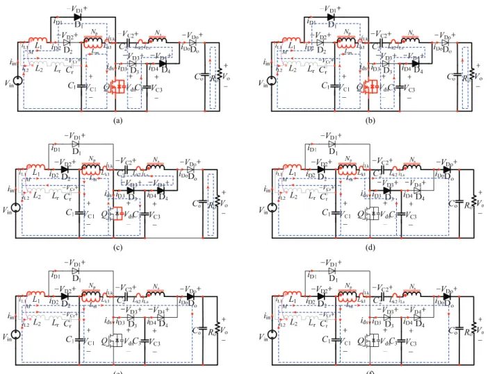
ONVERTER A diode-capacitor voltage multiplying unit and an input(a)
(b)
Fig. 1. High gain DC/DC converter with a ripple absorption circuit. (a) Circuit topology. (b) Topological equivalent circuit. current ripple absorption circuit are integrated into a QBC to obtain the circuit topology of a converter shown in Fig. 1(a). The main working circuit includes a DC input power supply
Vin, an active power switch tube Q, five diodes D1-D5, three
storage capacitors C1-C3, one output filter capacitor, two pairs
of coupled inductors T1-T2, and one weak voltage and current
ripple absorption circuit. The voltage multiplying unit (composed of diodes D3 and D4), the storage capacitor C2 and
the secondary side of the coupled inductor T2 can be used to
increase the voltage gain of the converter. The ripple absorption circuit is composed of the auxiliary inductor Lr,
the auxiliary capacitor Cr and the secondary side of the
coupled inductor T1. The input inductor L1 and the inductor L2
are assembled into one magnetic core to structure a coupled inductor that can reduce the amplitude of the input current ripple to a low level. The peak absorption circuit is composed of the parasitic capacitance of the switch Q, the clamping diode D3 and the capacitor C3. The maximum voltage across
the switch Q is clamped to the voltage of the capacitor C3. Fig.
1(b) shows a topology equivalent circuit of the converter. The coupled inductor T1 is a fully coupled inductor, where the
turns ratio can be expressed as N1(N1=(L1/L2)½). The mutual
inductance of T1 can be expressed as M. The coupled inductor
T2 can be equivalent to a high-frequency transformer with a
turns ratio of N2(N2=Ns/Np). In addition, the magnetizing
inductance is Lm, and the leakage inductance of the primary
and secondary sides are Lk1 and Lk2, respectively. In order to
simplify the circuit analysis and ignore the interference on the converter characteristics caused by the device parameters, the following assumptions should be made.
1) All of the capacitors in the circuit are large enough so that
Fig. 2. Working principle waveforms of the converter in a switching period.
the voltage ripples across both terminals can be ignored, and the voltage across all of the capacitors is constant in a switching period.
2) Except for containing the anti-parallel diode and capacitors, the switch tube and diodes are ideal devices without switching losses.
3) The coupled inductor T2 is a high-frequency transformer
considering the magnetizing inductance and leakage inductance, and its coupling coefficient is k2=Lm/(Lk1+Lm).
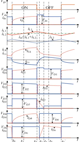
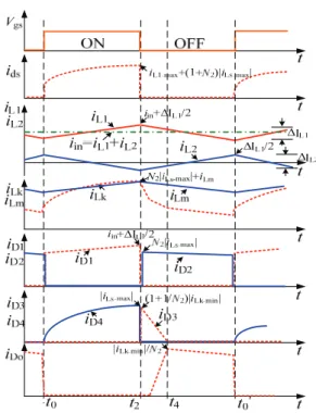
According to the above assumptions and the on-off states of the switch, the diode and the energy storage device, a converter operating in the continuous conduction mode (CCM) of the inductor current can be divided into six operating modes in a switching period. Modal equivalent circuits of the converter are shown in Fig. 3. Fig. 2 shows waveforms of the inductor current, the voltage and the current of the switching devices during a switching period. The modal switching process is as follows.
1) Mode 1[t0<t<t1, as shown in Fig. 3(a)]: At time t0, the
switch Q and the diodes D1 and D4 are turned on, and the
diodes D2, D3 and Do are turned off and supported by the
C1 D2 D1 Do Q Co Ro D3 C2 Np Ns L1 Lr Cr L2 * * M D4 C3 Vin Ripple absorption circuit Voltage spike absorption circuit Diode-capacitor voltage multiplying unit
(a) (b) (c) (d) (e) (f)
Fig. 3. Equivalent circuits of the proposed converter. (a) Mode 1. (b) Mode 2. (c) Mode 3. (d) Mode 4. (e) Mode 5. (f) Mode 6. reverse voltages VC1, VC3 and Vo,respectively. The energy
from the DC source Vin is delivered to the primary side
winding L1 through D1 and Q, and the current iL1 is linearly
enlarged. In this mode, iL1 is smaller than the effective value
of the input current, and the secondary side of T1 and the
auxiliary inductor Lr are charged by the auxiliary capacitor.
Meanwhile, the secondary side current iL2 of T1,which is
greater than zero, is opposite to the variation tendency of iL1.
As a result, the input current ripple is reduced. The energy storage in the capacitor C1 is released to the primary side of
T2 through Q, and the current iLk rises linearly. The energy
stored in the secondary side of T2 is transferred to the
capacitor C2 by using the transformer effect, and the current
iLs rises in the opposite direction.
(1)
(2)
(3)
(4)
(5)
2) Mode 2[t1<t<t2, as shown in Fig. 3(b)]: In this mode, the
switch Q and the diodes D1 and D4 continue to conduct, and
the diodes D2, D3 and Do are turned off. The energy from the
DC source Vin is released to the primary side of T1 via D1 and
Q, C1 is discharged to the primary side of T1 through Q, and
iL1 and iLk continue to rise. The secondary side of T2 and the
capacitor C3 are discharged to C2, and the current -iLs rises. iL1
is greater than the effective value of the input current. In addition, the current iL2 is opposite to iL1 and its amplitude is
less than zero. Therefore, the input current ripple is reduced by the sum of the ripples of the currents iL1 and iL1.
3) Mode 3[t2<t<t3, as shown in Fig. 3(c)]: In this mode, the
switch Q and the diode D1 are turned off, and the diode D2 is
continuously turned on. At t2, D3 with support from the
forward voltage is conducted and forms a discharge circuit with the parasitic capacitors of Q and C3. The voltage across
Q is clamped to the voltage of C3. The current path of iLk is
rapidly switched from the switch Q to C3. In addition, iLk
declines rapidly. The leakage energy in both sides of T2 is
stored in C2 via D4, and the current -iLs decreases linearly. in L1 L2 i i i L1 L2 1di di in L M V dt dt L1 L2 2 r in Cr C1 ( ) di di M L L V V V dt dt Lm 2 C1 V k V Ns C2 C3 V V V
(6)
(7)
4) Mode 4[t3<t<t4,as shown in Fig. 3(d)]: In this mode, the
switch Q and the diode D1 remain turned off, and the diode
D2 is conducted. At t3, the leakage inductance energy in both
sides of T2 is completely discharged. In addition, the diode D4
is turned off, and output diode Do is conducted. The energy
from the primary side of T1 and Vin is transferred to C1 via D2.
In addition, iL1 decreases linearly. The energy stored in the
primary side of T2 is released to C3 through D3, and
discharged to the output side through Do with the secondary
side of T2 and C2. In addition, iLk decreases linearly, and the
current iLs rises linearly. The current iL1 is greater than the
effective value of the input current, and Cr is charged by the
secondary side of T1 and the auxiliary inductor Lr. In addition,
iL2 rises linearly and its amplitude is less than zero.
(8)
(9)
(10)
(11)
5) Mode 5[t4<t<t5, as shown in Fig. 3(e)]: At t4, the storage
capacitor C3 is completely charged and the diode D3 is turned
off. In this period, Q and D1 are turned off, and D2 and Do are
conducted. The energy in the primary side of T1 is discharged
to C1 through D2, and iL1 maintains a downward trend. Cr is
charged by the secondary side of T1 and Lr, and the current
-iL2 continues to decrease. The energy stored in the secondary
side winding of T2 and C2 is released to the output load via Do.
In addition, the current iLk starts to rise, and the current iLs
begins to decline.
6) Mode 6[t5<t<t0′, as shown in Fig. 3(f)]: At t5, the current
iL1 is equal to the effective value of the input current and -iL2
drops to zero. In this mode, the primary side of T1 continues
to discharge, and iL1 declines lower than iin. Meanwhile, the
capacitance energy stored in Cr is discharged to the secondary
side of T1 and Lr, and iL2 begins to increase. The energy stored
in the secondary side winding of T2 and C2 is sequentially
released to the output load via Do, and the current iLk
continues to increase. Until time t0′, when switch is turned
back on, the converter starts the next switching period.
III. S
TEADYS
TATEA
NALYSISA. Voltage Gain
In order to reduce the volume of the magnetic component, the coupling inductor T1, the auxiliary inductor Lr and the
auxiliary capacitor Cr are combined to form a ripple
absorption circuit, which can reduce the ICR with the ripple suppression capability of the coupled inductor. T1 can be
configured as a fully coupled inductor, and its coupling coefficient can be expressed as:
(12)
During the two periods of the switch turn-on and turn-off, the voltage across the inductor can be approximately constant. In order to simplify the analysis process with the above mode analysis, the inductor voltage in modes 1 and 4 are used to represent the inductor voltage during the two periods of the switch turn-on and turn-off, respectively. In a switching period Ts, by using the volt-second balance law in two sides of T1 and the magnetizing inductance Lm of T2, the voltage of C1, C2, C3 and Cr can be obtained by arranging equations (2) - (5) and (8) - (11): (13)
(14)
(15)
(16)
Based on (10) - (11), the output voltage of the proposed converter can be expressed by: (17)
Therefore, the steady-state voltage gain of the converter can be obtained when the converter operates in the CCM: (18)
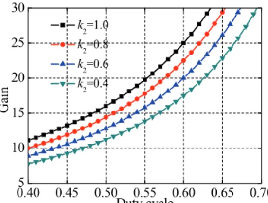
Fig. 4 shows gain contrast curves of the converter under different coupling coefficients. It is shown that the leakage inductance and the coupling inductance T1 have no effect on the voltage gain of the converter. However, the gain loss of the converter due to the leakage inductance of T2 cannot be ignored. Therefore, the design of coupling inductor T2 should ensure that the winding is compact and minimize the air gap between magnetic cores for to reduce the gain loss caused by the leakage inductance. When the gain loss caused by the leakage inductance in T2 is ignored (k2 =1), the voltage gain of the converter can be expressed as: (19) It can be obtained from equation (19) that the voltage gain of the converter is simultaneously controlled by the duty ratio
D and the turns ratio N2 of T2 without considering the
influence of the leakage inductance T2 on the gain. In other
words, increases of the duty cycle D and the turns ratio N2 can
enlarge the voltage gain of the converter. In high gain requirement applications, the gain of the converter can be
ds C3 V V 2 C1 C3 Lm m ( ) k V V di dt L L1 L2 1di di in C1 L M V V dt dt L1 L2 2 r C1 in Cr ( ) di di M L L V V V dt dt Lm 2( C1 C3) V k V V Ns C2 C3 o V V V V 1 1 2 M k L L in C1 1V V D in Cr 1DV V D C2 (1 ) o (1 2 ) C3 V D V D V C1 C3 1V V D o C2 2 2 C3 2 2 C1 2 2 in (1 ) 2 (1 ) V V k N V k N V k N V D o 2 2 2 2 CCM 2 in 2 ( , , ) (1 ) V k N G D N k V D 2 2 CCM 2 2 ( , ) (1 ) N G D N D
Fig. 4. Gain comparison curve under different coupling coefficients k2.
Fig. 5. Gain comparison curves with different turns ratios N2 and duty cycles.
further improved by increasing the turn ratio N2 without an
extremely high duty cycle.
B. Voltage Stress Analysis
According to the above analysis of the operation mode and steady-state gain, the voltage stress of the switching devices including the switch Q and the diodes D1-Do can be derived
from (13)-(16). Ignoring the influence of the voltage ripple on the capacitor C3 and the leakage inductance of the coupled
inductors, the voltage stress of the switch Q can be obtained from modes 3 and 4. The parameter measurement for the armature inductance L1 is also executed in a wide frequency
range from 40Hz to 100Hz under various V/f ratios. The armature inductance is calculated by using the center of the
P-Q circle diagram depicted for each driving frequency.
(20)
According to mode 1 and mode 3, the voltage stresses of diodes D1, D2 and D3 are (VC3-VC1), VC1 and VC3, respectively.
From mode 2 and mode 4, the voltage stresses of the diode D4
and the output diode Do are equal to (Vo-VC3). Therefore, the
voltage stress expressions of D1 and Do can be expressed as:
(21)
Fig. 6. Ratio of the diode voltage to the output voltage under different turns ratios and duty cycles.
(22) (23) (24) Fig. 6 shows variation curves of the ratio of the voltage on the diode and the output under different turn ratios and duty cycles. It is noticeable that the voltage stress of the diode D1
is proportional to the duty cycle D and inversely proportional to the turn ratio N2. The voltage across the diode D2 is
inversely proportional to D and N2. When the voltage spikes
of the switching tube are ignored, the voltage stress of the diode D3 is equal to the voltage across the switching tube, and
the ratio VD3/Vo is independent of D and proportional to N2.
The voltages across the diodes D4 and Do are equal, and the
ratio VD4/Vo is independent from D and rises with an increase
of N2. Therefore, when the input voltage and output voltage
are constant, the duty cycle and the turn ratio N2 should be
reasonably allocated to effectively reduce the voltage stress of the switching devices and to improve the efficiency of the converter.
C. Current Stress Analysis
In order to simplify the current stress analysis of switching devices, the simplified current stress diagram shown in Fig. 7 can be obtained by neglecting the leakage inductance influence. According to equations (2) and (3), the current ripple of the inductors L1 and L2 can be expressed as:
(25) (26) According to operating modes 1 and 2, the input current is equal to the sum of the current flowing through L1 and L2. In
order to make the ICR as small as possible, it is necessary to properly configure the current ripple of L2. When the absolute
0.405 0.45 0.50 0.55 0.60 0.65 0.70 10 15 20 25 30 Ga in Duty cycle k2=1.0 k2=0.8 k2=0.6 k2=0.4 0.3 0.4 0.5 0.6 0.7 0.8 0 20 40 60 80 Gai n Duty cycle N2=1 N2=2 N2=3 N2=4 o in ds C3 2 2 2 (1 ) V V V V N D o in D1 C3 C1 2 2 2 (1 ) DV DV V V V N D 0.2 0.3 0.4 0.5 0.6 0.7 0.8 -0.1 0.0 0.1 0.2 0.3 0.4 0.5 0.6 0.7 0.8 0.9 N2=2 N2=3 N2=4 o in D2 C1 2 (1 ) 1 2 D V V V V D N o in D3 C3 2 2 2 (1 ) V V V V N D 2 o D4 Do o C3 2 (1 ) 2 N V V V V V N 2 r in in Cr C1 L1 2 s 1 2 r ( ) ( ) ( ) L L V M V V V i DT L L L M 1 in Cr C1 in L2 2 s 1 2 r ( ) | | ( ) L V V V MV i DT L L L M
Fig. 7. Device current stress simplified diagram.
value of the current ripple ΔiL2 is equal to thecurrent ripple
ΔiL1 in same time and the variation tendency is opposite, very
small input current ripples that are close to zero can be achieved. Therefore, the current stress of L1 and L2 are
obtained as:
(27) (28) By using the ampere-second balance law in the capacitor
C1, the average current flowing through the primary winding
of T2 is zero in a switching period. The current iLk is equal to
the superposition of the current flowing through the secondary winding and the magnetizing inductor current of T2.
Thus, the following can be obtained:
(29)
(30) From the current flowing path of the diodes and the current stress of all the inductors, the current stress of D1 and D2 can
be expressed as follows:
(31)
(32) According to mode 2 and mode 4, the current flowing through the diodes D3, D4 and Do varies with the change of
the current flowing through the secondary winding of T2.
Therefore, the current stresses of D3, D4 and Do are obtained
as follows:
(33)
(34)
(35) As shown in Fig. 7, the current stress of the switch is equal to the current of the switch at time t2. At this time, the
charging process of L1 and the magnetizing inductance of T2
is completed. Therefore, the current stress of the switch can be written as follows:
(36)
D. Realization Conditions for Zero Ripple of the Input Current
Very small ripples of the input current can be achieved due to the ripple-suppressed capabilities of the coupled inductor. According to the above current stress analysis of L1 and L2,
very small input current ripples that are close to zero can be obtained when the absolute value of the current ripple ΔiL2 is
equal to thecurrent ripple ΔiL1 in same time and the variation
tendency is opposite. Hence, the detailed derivation process of the realization condition for zero ripple of the input current is expressed as follows.
As can be seen from Fig. 7 and from equations (25)-(26), the following can be obtained:
(37)
Without considering the influence of capacitor voltage ripples, substituting equations (13) - (14) into equation (37) yields:
(38) Assume the coupling coefficient k1 of the coupled inductor
T1 is 1, that is M=(L1L2)½, the condition can be obtained by
equation (38) as follows:
(39) Therefore, by using a ripple absorption circuit composed of a coupled inductor T1, an auxiliary inductor Lr and an auxiliary
L1 2 L1 L1-max 2 2 2 o 2 (1 ) in i N i i i I D L1 L2-max 2i i 2 o C1 Lm-max Lk-max 2 m s (2 ) 2 (1 ) N I V D i i L f D 2 o C1 Lm-min 2 m s (2 ) 2 (1 ) N I V D i L f D 2 L1 D1-stress L1-max 2 2 o 2 (1 ) N i i i I D 2 L1 D2-stress L1-max 2 2 o 2 (1 ) N i i i I D D3-stress Lk Lk Lm 2 2 2 o C1 2 2 m s 2 1 ( ) ( 1)(2 ) 2 (1 ) i i i i N N N I V D N L f N D 2 o C1 D4-stress Ls-max 2 2 m s 2 (2 ) | | 2 (1 ) N I V D i i N L f N D 2 o C1 Do-stress Ls-max 2 2 m s 2 (2 ) | | 2 (1 ) N I V D i i N L f N D 2 r = + M L L
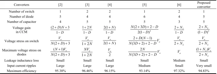
TABLE I
COMPARATIVE ANALYSIS OF CHARACTERISTICS
Converters [2] [3] [4] [5] [6] converterProposed
Number of switch 1 2 2 1 2 1
Number of diode 5 4 4 6 4 5
Number of capacitor 4 5 5 5 3 5
Voltage gain in CCM Voltage stress on switch Maximum voltage stress on
diodes
Leakage inductance loss Small Small Small Small Medium Small
Input current ripples Large Large Large Medium Small Very small
Maximum efficiency 95.38% 96.46% 96.15% 93.14% 97.32% 94.83%
Fig. 8. Voltage gain comparison with N2=2.
Fig. 9. Ratios between the diode voltage and the output voltage. capacitor Cr, very small ripples of the input current can be
achieved by reasonably configuring the turn ratio of the primary and secondary inductors T1 and the value of auxiliary
inductor Lr to satisfy equations (37)-(38).
IV. C
ONVERTERC
HARACTERISTICSC
OMPARISON In this paper, a number of DC/DC converters with high gains and low switching voltage stresses are selected for a comparative analysis with the proposed converter. Table Igives a comparative analysis of the main performances and experimental results among the converters, including the number of devices, voltage gain, voltage stress of switch, maximum voltage stress of diode, leakage loss, input current ripple and maximum efficiency. Fig. 8 shows a gain comparison among some homothetic converters. Fig. 9 shows a voltage stress comparison of the switching tube when the turns ratios are equal. In addition to a high voltage gain and a low voltage stress, the converter proposed in this paper can achieve zero ripple of the input current.
V. P
ARAMETERD
ESIGNIn order to verify the steady-state characteristics of the converter and the feasibility of the theoretical analysis, an experimental prototype is designed in this paper. The parameters of the experimental prototype are designed as follows.
1) Input voltage range Vin= 18V-36V.
2) Output voltage Vo= 400V.
3) Rated output power Po= 200W.
4) Switching frequency fs= 40kHz.
A. Selection of the Duty Cycle and Turn Ratio N2
According to equation (18) and considering the gain loss due to the leakage inductance of the coupled inductor, the voltage gain can step up in order meet the requirement of the experimental prototype when the input voltage is 18V, the value of N2 is 3, and the duty ratio is 0.54.
B. Selection of the Inductors L1, L2, Lr and Turn Ratio N2
According to the above analysis of the input current ripples, the inductor L1 should be large enough to ensure that its
minimum current is greater than zero. The primary side equivalent inductance of the coupled inductor T1 is larger
than the value of L1 when an independent inductance is used.
In order to obtain a continuous inductor current, L1 should be
(2 ) 3 1 D N D 1 2 1 N D 2(1 ) 1 N D 2 (2 3 ) 2 2(1 ) N D D D 2 2 1 N D 2 2 2 (1 ) N D (2 ) 3 o V N D 1 2 o V N 2(1 ) o V N 2 ( 1) (3 2) 2 o D N V N D D 2 2 o V N 2 2 o V N ( 1) (2 ) 3 o N V N D 1 2 o NV N 2 o V 2 (3 2) 2 o N V N D D Vo 2 2 (1 ) 2 o N V N 0.0 0.1 0.2 0.3 0.4 0.5 0.6 0.7 0.8 0 10 20 30 40 [2] [3] [4] [5] [6] Proposed converter Duty Cycle Voltag e Ga in 0.1 0.2 0.3 0.4 0.5 0.6 0.7 0.8 0.9 0.0 0.1 0.2 0.3 0.4 0.5 0.6 [2] [3] [4] [5]
Proposed conveter and [6]
Duty Cycle
Vds
/V
selected as follows:
(40) Therefore, the primary inductance value of T1 is 240μH.
According to equation (39), it is necessary to satisfy N1>1 to
achieve zero ripple of the input current. Therefore, N1 can be
set to 2. Assuming the coupled inductor is a fully coupled inductor, the value of the secondary side L2 of T1 can be
obtained as follows:
(41) Since the leakage inductance of the coupled inductor cannot be ignored, it can be obtained according to equation (38) as follows:
(42) Therefore, the auxiliary inductance Lr is selected to be
58μH.
C. Selection of the Magnetizing Inductance Lm
To operate the converter in the CCM mode of the inductor current, the minimum value of the magnetizing inductor
current iLm needs to be greater than zero. According to
formula (30), Lm needs to satisfy the following relational
expression:
(43)
Therefore, Lm can selected to be 200μH, which can ensure
that the inductance current operates in the CCM without increasing the number of turns of T2 and reducing the volume
of the magnetic components.
D. Selection of the Switch and the Diode
The rated voltage of the switching devices can be obtained based on (20)-(24) and (31)-(36). In practice, voltage spikes can be triggered during the switching transition process. Hence, FQP34N20 (200V, 31A, 0.075Ω) can be used for the switch, Schottky diodes MBR20200 (200V, 20A) can be used for the diodes D1 and D2, and fast recovery diodes SFF1606G
(400V) can be used for the diodes D3, D4 and Do.
E. Selection of the Capacitor
The rated voltage of the capacitors can be obtained from (13)-(16). The selected capacitor capacity needs to be greater than 1.5 times the theoretical value to reduce voltage ripples. In addition, the values of the capacitors are supposed to satisfy the following condition:
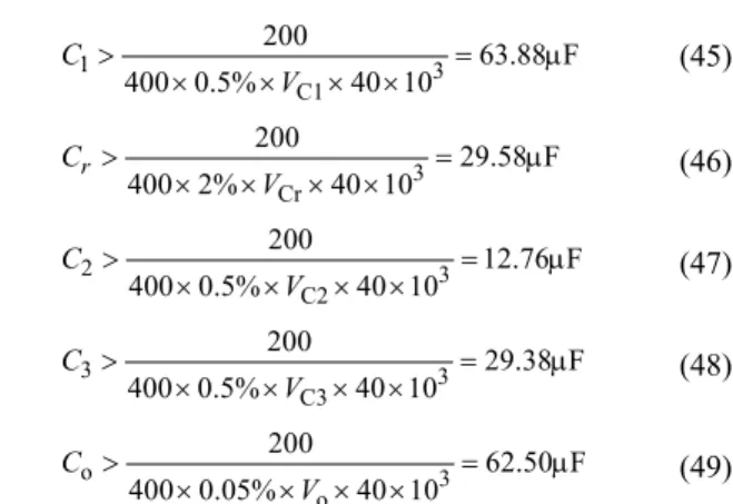
(44) Therefore: (45) (46) (47) (48) (49)
The capacitor C1, as the equivalent excitation power of T1
should maintain stability. Therefore, its parameters can be selected as 100μF and 100V. In order to reduce the output voltage ripple, the output capacitor Co is selected to be an
electrolytic capacitor with parameters of 470μF/450V, the auxiliary capacitor is selected with parameters of 22μF/ 50V, and C2 and C3 are selected with parameters of 47μF/ 250V.
VI. S
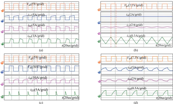
IMULATIONR
ESULTSFig. 10 shows waveforms of simulation results under the same parameters as the experimental prototype, including the voltage and current waveforms of the switch, and the current waveform of the diodes and inductors. It can be observed from the results that the input current ripple is approximately zero. When the input voltage and output voltage are 18V/400V, the turns ratio N2 is 3 and the duty ratio is 0.54,
the switching tube voltage stress is about 80V. The simulation results are basically consistent with the principle analysis.
VII. E
XPERIMENTALR
ESULTSAn experimental prototype has been constructed to verify the feasibilities of the proposed converter by using the design parameters in this paper. Sampled waveforms are presented in Fig. 11(a) including waveforms of the driving pulse, and current waveforms of the input and the two sides of T1. The
ripple absorption circuit, composed of a coupled inductor T1,
an auxiliary inductor Lr and an auxiliary capacitor, can reduce
the input current ripple. This can be seen from the fact that
the current variation tendency of the two sides of T1 is
opposite. By adjusting the auxiliary inductance, the peak-to- peak value of the input current ripples can be reduced to lower than 5%.
Fig. 11(b) illustrates the gate signal of Q and the current
waveform of T2. Figs. 11(c) and 11(d) show current
waveforms of all the diodes and the switch tube. Obviously,
when the switch is turned off, the primary current of T2
decreases, and the diodes D3 and D4 are conducted. In
in 1 3 in s 18 0.54 21.87 H 100 2 2 40 10 18 V D L i f 1 2 2 1 240 = 60 H 4 L L N 1 2 2 < 60 H r L L L L o o C s P C V V f 1 3 C1 200 63.88 F 400 0.5% 40 10 C V 3 Cr 200 29.58 F 400 2% 40 10 r C V 2 3 C2 200 12.76 F 400 0.5% 40 10 C V 3 3 C3 200 29.38 F 400 0.5% 40 10 C V o 3 o 200 62.50 F 400 0.05% 40 10 C V
(a) (b)
(c) (d)
Fig. 10. Simulation test waveforms.(a) Vgs, iD1, iD2 and iDo.(b) Vgs, iin, iL1 and iL2.(c) Vgs, Vds, ids and iD3. (d) Vgs, iLk, iLs and iD4.
(a) (b) (c)
(d) (e) (f)
Fig. 11. Experimental prototype test waveforms.(a) Vgs, iin, iL1 and iL2.(b) Vgs, iLk and iLs.(c) Vgs, iD1, iD2 and iD3. (d) Vgs, ids, iD4 and iDo.
(e) Vgs, VD1, VD2 and VDo.(f) Vds, Vin, Vo and VCr with Vin=18V.
addition, the energy stored in the primary and secondary side leakage inductances of T2 is recovered into the capacitors C3
and C2 and eventually to the load. The diodes D1 and D2 are
conducted in the complementary mode. Hence, they can provide loops for the charge and discharge processes of the coupled inductor T1, which can improve the voltage gain of
the converter.
As can be seen from Fig. 11(d), the output voltage can be step up to 400V when the input voltage is 18V, and the current stress of the switch is about 10A, which is consistent with the theoretical analysis and simulation test results.
Fig. 11(e) gives the gate signal of Q and voltage waveform of the diodes D1, D2 and Do. It is easy to observe that the
output diode can achieve approximately zero voltage switching
Vgs(5V/grid) iD1(5A/grid) iD2(5A/grid) iDo(1A/grid) t(20us/grid) Vgs(5V/grid) Vds(50V/grid) ids(10A/grid) iD3(5A/grid) t(20us/grid) Vgs(7.5V/grid) iLk(5A/grid) iLs(2A/grid) iD4(0.5A/grid) t(20us/grid)
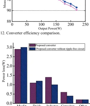
Fig. 12. Converter efficiency comparison.
Fig. 13. Loss distribution of devices.
(ZVS). When the diode D3 is turned off, the voltage across
the diode D3 is clamped at a low voltage (VNs+VC2-VD4). In
addition, the voltage across the diode D1 has a voltage drop at
the same time.
Fig. 11(f) illustrates waveforms of the output voltage, the switching voltage and the voltage across the auxiliary capacitor Cr when the input voltage is 18V. The voltage stress
of the switch is about 80V and the voltage across the auxiliary capacitor is only about 20V. Voltage spikes of the switch can be suppressed by a passive lossless absorption circuit composed of a diode D3 and a capacitor C3 at the
moment of switching turn off. The current flowing through the ripple absorption circuit current is very small. Therefore, this auxiliary branch can be constructed by a capacitor and litz wire with a low tolerance parameter to reduce the place of the converter.
Fig. 12 shows an efficiency comparison of the proposed converter and a converter without a ripple absorption circuit under different loads. As can be seen from Fig. 13, the proposed converter with a ripple absorption circuit contains additional conduction loss due to the auxiliary capacitance and inductance. In addition, the switching device loss and the energy storage device loss of the proposed converter are lower than the converter without a ripple absorption circuit. Therefore, the conversion efficiency of the converter proposed
in this paper is slightly lower than the high gain converter without a ripple absorption circuit. The maximum efficiency of the high gain converter without a ripple absorption circuit is 95.82%, and proposed high gain converter proposed achieves a maximum efficiency of 94.83% when the power is Po=60W. Nevertheless, a very small input ripple that is
close to zero can be obtained from the high gain converter proposed in this paper, which can provide a good alternative option with attractive performance for some occasions such as PV generation systems.
VIII. C
ONCLUSIONIn this paper, a double-coupled inductor high gain DC/DC converter with a ripple absorption circuit is proposed. When compared with a traditional quadratic high gain converter and a coupled inductor high gain converter, the proposed converter has the following advantages. 1) A voltage multiplier module composed of a diode-capacitor unit and a coupled inductor is integrated into a conventional converter, and a higher voltage gain can be obtained by configuring the turns ratio of the coupled inductor and the duty ratio, which can effectively avoid an extremely high duty cycle and reduce the leakage inductance loss caused by the weak coupling of a high frequency transformer. 2) Very small input current ripples can be achieved by using a ripple absorption circuit composed of an auxiliary inductor and a capacitor, which effectively reduces the switching devices loss. Additionally, the current through the ripple absorption circuit is small and the volume of the absorption branch is tiny. 3) The voltage stress of the switch tube can be clamped at a value much lower than the output voltage since the voltage across the switch and the output voltage are isolated by the voltage multiplying unit. 4) The leakage inductance loss of the coupled inductor can be recovered and fed back to the load in a switching period, which can improve the efficiency of the converter.
A
PPENDIXThis appendix provides the approximate derivation used to estimate the loss breakdown in the proposed converter [14]. The loss in the active switch is mainly conduction losses [32]. The conduction losses are estimated using the RMS current through the switch and its on-state resistance. Thus, the losses in the active switch Q are given by:
(50) where Irms is the RMS current through the switch Q, and Rds-on
is its on-state resistance.
The diode losses can be obtained by:
(51) 0 50 100 150 200 250 88 90 92 94 96 98 Proposed converter
Proposed converter without ripple-free circuit
Output Power(W)
Me
asured
Efficiency
(%)
Mosfet Doide Inductor Capacitor Other 0.0 0.5 1.0 1.5 2.0 2.5 3.0 Po wer lo ss (W) Proposed converter
Proposed converter without ripple-free circuit
2 rms ds-on Q P I R 2 diode rms-d T avg-d T P I R I V
where Irms-d is the RMS current through the diode, RT is its
on-state resistance, Iavg-d is its average current, and VT is its
on-state voltage drop.
The capacitor losses are estimated by using the following equation:
(52)
where Irms-c is the RMS current through the capacitor and RESR
is its equivalent series resistance.
The losses in the magnetic components are comprised of the core losses and the winding losses [10]. The core losses are estimated as:
(53)
where k is the eddy current loss coefficient, Bac is the
magnetic flux variation, and Wtfe is the core weight in grams.
The winding losses in T1, T2 and Lr are estimated by using
the following equation:
(54)
where Irms-cuis the RMS current through the wire, and Rcu is
the resistance of the wire.
R
EFERENCES[1] K. C. Tseng and C. C. Huang, “High step-up high-efficiency interleaved converter with voltage multiplier module for renewable energy system,” IEEE Trans. Ind. Electron., Vol. 61, No. 3, pp. 1311-1319, Mar. 2014.
[2] T. J. Liang and J. H. Lee, “Novel high-conversion-ratio high efficiency isolated bidirectional dc-dc converter,”
IEEE Trans. Ind. Electron., Vol. 62, No. 7, pp. 4492-4503,
Jul. 2015.
[3] K. C. Tseng, C. C. Huang, and C. A. Cheng, “A single- switch converter with high step-up gain and low diode voltage stress suitable for green power-source conversion,”
IEEE J. Emerg. Sel. Topics Power Electron., Vol. 4, No.
2, pp. 363-372, Jun. 2016.
[4] A. Mustafa Al-Saffar and E. H. Ismail, “A high voltage ratio and low stress dc–dc converter with reduced input current ripple for fuel cell source,” Renew. Energy, Vol. 82, pp. 35-43, Oct. 2015.
[5] G. Wu, X. B. Ruan, and Z. Ye, “Non isolated high step-up dc–dc converters adopting switched-capacitor cell,” IEEE
Trans. Ind. Electron., Vol. 62, No. 1, pp. 383-393, Jan.
2015.
[6] Y. Tang, T. Wang, and D. Fu, “Multi cell switched-inductor/ switched-capacitor combined active-network converters,”
IEEE Trans. Power Electron., Vol. 30, No. 4, pp. 2063-
2072, Apr. 2015.
[7] B. X. Zhu, S. Cheng, and C. Tan, “ZVS isolated high step-up dc/dc converter,” Electric Power Automation
Equipment, Vol. 35, No. 5, pp. 70-76, May 2015.
[8] S. W. Lee and H. L. Do, “Isolated Sepic dc-dc converter with ripple-free input current and lossless snubber,” IEEE
Trans. Ind. Electron., Vol. 65, No. 2, pp. 1254-1262, Feb.
2018
[9] T. J. Liang and J. H. Lee, “Novel high-conversion-ratio high-efficiency isolated bidirectional dc-dc converter,”
IEEE Trans. Ind. Electron., Vol. 62, No. 7, pp. 4492-4503,
Jul. 2015.
[10] T. J. Liang, J. H. Lee, S. M. Chen, J. F. Chen, and L. S. Yang, “Novel isolated high-step-up dc-dc converter with voltage lift,” IEEE Trans. Ind. Electron., Vol. 60, No. 4, pp. 1483-1491, Apr. 2013.
[11] Y. H. Hu and W. D. Xiao, “Three-port DC-DC converter for stand-alone photovoltaic systems,” IEEE Trans. Power
Electron., Vol. 30, No. 6, pp. 3068-3076, Jun. 2015.
[12] T. J. Liang and J. H. Lee, “Novel high-conversion-ratio high efficiency isolated bidirectional dc-dc converter,”
IEEE Trans. Ind. Electron., Vol. 62, No. 7, pp. 4492-4503,
Jul. 2015.
[13] J. H. Lee, T. J. Liang, and J. F. Chen, “Isolated coupled- inductor integrated dc-dc converter with nondissipative snubber for solar energy applications,” IEEE Trans. Ind.
Electron., Vol. 61, No. 7, pp. 3337-3348, Jul. 2014.
[14] M. Kim and S. Choi, “A fully soft-switched single switch isolated dc-dc converter,” IEEE Trans. Power Electron., Vol. 30, No. 9, pp. 4883-4890, Sep. 2015.
[15] K. C. Tseng, C. C. Huang, and C. A. Cheng, “A high step-up converter with voltage-multiplier modules for sustainable energy applications,” IEEE J. Emerg. Sel. Topics Power
Electron., Vol. 3, No.4, pp. 1100-1108, Dec. 2015.
[16] N. K. Reddi, M. R. Ramteke, H. M. Suryawanshi, K. Kothapalli, and S. P. Gawande, “An isolated multi-input ZCS DC-DC front-end-converter based multilevel inverter for the integration of renewable energy sources,” IEEE
Trans. Ind. Electron., Vol.54, No. 1, pp. 494-504, Jan/Feb.
2017.
[17] H. W. Liu, H. Hu, H. Wu, Y. Xin, and I. Batarseh, “Overview of high-step-up coupled-inductor boost converters,” IEEE J. Emerg. Sel. Topics Power Electron., Vol. 4, No. 2, pp. 689-704, Jun. 2016.
[18] Y. Deng, Q. Rong, W. Li, Y. Zhao, J. Shi, and X. He, “Single-switch high step-up converters with built-in transformer voltage multiplier cell,” IEEE Trans. Power
Electron., Vol. 27, No. 8, pp. 3557-3567, Aug. 2012.
[19] K. C. Tseng, C. C. Huang, and C. A. Cheng, “A single- switch converter with high step-up gain and low diode voltage stress suitable for green power-source conversion,”
IEEE J. Emerg. Sel. Topics Power Electron., Vol. 4, No.
2, pp. 363-372, Jun. 2016.
[20] W. Li, W. Li, X. Xiang, Y. Hu, and X. He, “High step-up interleaved converter with built-in transformer voltage multiplier cells for sustainable energy applications,” IEEE
Trans. Power Electron., Vol. 29, No. 6, pp. 2829-2836, Jun.
2014.
[21] S. Sathyan, H. M. Suryawanshi, B. Singh, C. Chakraborty, V. Verma, and M. S. Ballal, “ZVS-ZCS high voltage gain integrated Boost converter for dc microgrid,” IEEE Trans.
Ind. Electron., Vol. 63, No. 11, pp. 6898-6908, Nov.
2016.
[22] A. Ajami, H. Ardi, and A. Farakhor, “A novel high step-up dc/dc converter based on integrating coupled inductor and
2 capacitor rms-c ESR P I R 1.23 2.12 13 core ( s ac )( tfe)(10 ) P kf B W 2 cu-wire rms-cu cu
P
I
R
switched capacitor techniques for renewable energy applications,” IEEE Trans. Power Electron., Vol. 30, No. 8, pp. 4255-4263, Aug. 2015.
[23] M. Das and V. Agarwal, “Design and analysis of a high- efficiency DC–DC converter with soft switching capability for renewable energy applications requiring high voltage gain,” IEEE Trans. Ind. Electron., Vol. 63, No. 5, pp. 2936-2944, May 2016.
[24] X. F. Hu and C. Y. Gong, “A high voltage gain dc-dc converter integrating coupled-inductor and diode-capacitor techniques,” IEEE Trans. Power Electron., Vol. 29, No. 2, pp. 789-800, Feb. 2014.
[25] S. W. Lee and H. L. Do. “Zero-ripple input current high step-up Boost-SEPIC dc-dc converter with reduced switch voltage stress,” IEEE Trans. Power Electron., Vol. 32, No. 8, pp. 6170-6177. Aug. 2017.
[26] S. K. Changchien, T. J. Liang, J. F. Chen, and L. S. Yang, “Novel high step-up dc-dc converter for fuel cell energy conversion System,” IEEE Trans. Ind. Electron., Vol. 57, No. 6, pp. 2007-2017, Jun. 2010.
[27] P. Saadat and K. Abbaszadeh, “A single switch high step up dc-dc converter based on quadratic Boost,” IEEE Trans.
Ind. Electron., Vol. 57, No. 6, pp. 7733-7742, Dec. 2016.
[28] S. M. Chen, T. J. Liang, L. S. Yang, and J. F. Chen, “A cascaded high step-up dc-dc converter with single switch for microsource applications,” IEEE Trans. Power
Electron., Vol. 26, No. 4, pp. 1146-1153, Apr. 2011.
[29] X. F. Hu and C. Y. Gong, “A high gain input-parallel output-series dc/dc converter with dual coupled inductors,”
IEEE Trans. Power Electron., Vol. 30, No. 3, pp. 1306-
1317, Mar. 2015.
[30] P. Wang, L. Zhou, J. Li, Y. Zhang, and S. Mark, “Input- parallel output-series dc-dc Boost converter with a wide input voltage range for fuel cell vehicles,” IEEE Trans. Veh. Technol., Vol. 66, No. 9, pp. 7771-7781, Sep. 2017.
[31] P. Chavoshipour Heris, Z. Saadatizadeh, E. Babaei, and M. Sabahi, “New high step-up two-input-single-output converter with low-voltage stresses on switches and zero input currents ripple,” IET Power Electron., Vol. 11, No. 14, pp. 2241-2252, Oct. 2018.
[32] L. Schmitz, D. C. Martins, and Coelho R F, “Generalized high step-up dc-dc boost-based converter with gain cell,”
IEEE Trans. Circuits Syst. I, Reg. Papers., Vol. 64, No.
2, pp. 480-493, Feb. 2017.
[33] J. C. Rosas-Caro, F. Mancilla-David, J. C.Mayo-Maldonado, J. M. Gonzalez-Lopez, H. L. Torres-Espinosa, and J. E. Valdez-Resendiz, “A transformer-less high-gain boost converter with input current ripple cancelation at a selectable duty cycle,” IEEE Trans. Ind. Electron., Vol. 60, No. 10, pp. 4492-4499, Oct. 2013.
[34] Z. Y. Chen, Q. Zhou, and J. P. Xu, “Coupled-inductor boost integrated flyback converter with high-voltage gain and ripple-free input current,” IET Power Electron., Vol. 8, No. 2, pp. 213-220, Feb. 2015.
[35] A.J. Sabzali, E. H. Ismail, and H. M. Behbehani, “High voltage step-up integrated double Boost–Sepic dc–dc converter for fuel-cell and photovoltaic applications,”
Renew Energ., Vol. 82, pp. 44-53, Oct. 2015.
Jie Yang received his B.S. degree from the
School of Electronic and Information Engineering, Changchun University, Changchun, China, in 2014; and his M.S. degree from the School of Electrical and Power Engineering, China University of Mining and Technology, Xuzhou, China, in 2017. He is presently working as a Senior Engineer in the State Grid Linyi Power Supply Company, Linyi, China. His current research interests include power electronics, power system and electric drives.
Dongsheng Yu (M'14) received his B.S. and
Ph.D. degrees from the School of Information and Electrical Engineering, China University of Mining and Technology, Xuzhou, China, in 2005 and 2011, respectively. From 2009 to 2010, he was a Visiting Student with the University of Western Australia, Perth, WA, Australia, where he was an Endeavour Research Fellow, in 2014. He is presently working as an Associate Professor in the School of Electrical and Power Engineering, China University of Mining and Technology. His current research interests include power electronics, renewable energy, electric drives, nonlinear dynamics and memristive systems. He has published two books and over 30 papers in these areas.
Mohammed Alkahtani was born in Arrayn,
Saudi Arabia. He received his B.S. (Hons) degrees in Electrical and Electronics Engineering and his M.S. degree in Electrical Power and Control Engineering from the Liverpool John Moores University, Liverpool, ENG, UK, in 2014 and 2016, respectively. He is presently working towards his Ph.D. degree at the University of Liverpool, Liverpool, ENG, UK. His current research interests include soiling management of photovoltaics and PV array efficiency improvements.
Ligen Yuan was born in Taian, China. He
received his B.S. degree from the School of Electrical and Power Engineering, China University of Mining and Technology, Xuzhou, China, in 2018, where he is presently working towards his M.S. degree in the School of Electrical and Power Engineering. His current research interests include power electronic converters.
Zhi Zhou was born in China, in 1991. She
received her B.S. degree from the School of Electrical and Mechanical Engineering, Jinling Institute of Technology, Nanjing, China, in 2015; and her M.S. degree from the School of Electrical and Power Engineering, China University of Mining and Technology, Xuzhou, China, in 2018. She is presently working as a Senior Engineer in the State Grid Shanghai Qingpu Electric Power Supply Company, Shanghai, China. Her current research interests include memory components and microgrid systems.
Hong Zhu was born in Xuzhou, China. She
received the B.S. degree from the School of Electronic Engineering, Nantong University, Nantong, China, in 2014; and her M.S. degree from the School of Electrical and Power Engineering, China University of Mining and Technology, Xuzhou, China, in 2017. She is presently working for the State Grid Anhui Maintenance Company, Hefei, China. Her current research interests include DC-microgrids, AC/DC bidirectional converters and energy coordination control.
Maxwell Chiemeka was born in Uyo, Akwa
Ibom State, Nigeria. He received his Higher National Diploma degree in Electrical and Electronics Engineering from the Federal Polytechnic Nekede, Owerri, Imo State, Nigeria, in 2016. He is presently working towards his M.S. degree in Electrical Engineering at the China University of Mining and Technology, Xuzhou, China. His current research interests include memristor based filters in power line communications and power electronics.