A development of noise improvement dc-dc converter for PM OLED module
Sung-Joon Park*★
Abstract
In this paper, analysis of a noise factor and an effective power strategy for the OLED dc-dc converter are described. One of the main reasons that one may not design the OLED power for dc-dc converter is that OLED's panel noise is composed of FFN(Frame Frequency Noise) and LFN(Line Frequency Noise). Into the bargain, FFN is caused by both the dc-dc (circuit) and driving circuit. It is hard to get rid of FFN, baeause FFN has very little results value for our ears. LFN is adjusted by analog compensation value. Actually, that is more important problem than FFN. It is known that voltage divider for OLED's mode variation is not good for compact power design. In the end, a circuit design for understanding OLED's noise and a novel muti-channel dc-dc converter were presented.
Key words: PM OLED, dc-dc converter, OLED noise improvement circuit,
* Power Generation Division, Korea Hydro-Nuclear Power
★Corresponding author
Manuscript receved May. 25, 2009 ; receved Jun. 29, 2009
I. Introduction
This is great interest in OLED (organic light emitting display) technology for advanced displays because it is very thin, has a wide viewing angle and a fast response, uses low power and is lightweight. (OLED also has very fast response time, enabling a simple matrix addressing to be effectively used even for displaying fast moving pictures.) Plenty of products using our OLED at the marketplace include Cellular phone, MP3, and Photo CD burner[1-2].
Above all, OLED is an active emissive device. For the practical application of OLED, an important objective is to design the device's dc-dc converter.
It is relative to device's size, power consumption and luminance. Also the OLED's dc-dc converter has recently been considered as one of the key(s) points to improve the performance of OLED.
There are many power ICs available to design
LCD-module, but it is not easy to find adequate power IC for OLED's application.
If the power of dc-dc converter were insufficient, EL module would sensitively respond by input current. Moreover, in passive OLED, high efficiency, simple size, low temperate power converter are required.
The OLED's driving power are divided into dc (power) and ac power. We have developed the digital adjusting mode change scheme to improve the output current uniformity for PM(Passive Matrix) OLED. Also, we proposed the layout to reduce the noise between panel and dc-power portion. The novel dc-dc converter does not utilize MOS-FET for voltage divider and digital pulse counting method.
This new technique have several advantages. In previous systems, in order to prevent panel brightness from sunlight, we used the mode change method in proportion to sunlight. This is a method to step the brightness leading to sunlight. But, this system has some problems in using FET. However, (for) using digital pulse counting method, it is can be fast response, small size, economic COF's drawing. Also, it is very easy to control module's
mode as adjusting pulse generator.
II. Panel Design
We developed passive matrix 1.98-in. Average brightness and resolution of the sample panel are 50cd/㎡ and 120 × 160, and it drives with PWM(Pulse-width-modulation) and PFM(Pulse-frequ ency - modulation). We developed scaning duty-ratio is available to select freely. But average scaning duty is 1/60 cycle. Stack type column of anode pattern was formed in the active area by conventional photo-lithography technique. Before cathode separators are formed, a series of organic layers are formed on the top of ITO by the vapor deposition in vacuum.
Eventually, it has the organic layers were thermally deposited on the substrate with ITO film. Glass size is the 33.4×47.1(mm). The deposed Al sealing line is 0.38(mm). Dot pitch is 0.226×0.255(mm)[3].
We fabricated a ITO 1500Å, Mo 2600Å, Al 1500Å under standard conditions. We changed the thickness of electrode, we measured a result.
Scan(m) Scan(m+1)
Is
Level shifter
HVDD HVDD
PM OELD Panel GND
N-th data line driver
Date(n) Data(n+1) DEN
DEN
SiN
GND m-th scan line driver
HP2 HP1 HN2
HN3 HP4
Scan(m) Scan(m+1)
Is Is
Level shifter
HVDD HVDD
PM OELD Panel GND
N-th data line driver
Date(n) Data(n+1) DEN
DEN
SiN
GND m-th scan line driver
HP2 HP1 HN2
HN3 HP4
Fig. 1. Electrical model of an OLED pixel.
Ⅲ. Driving & controller circuit
OLED display can be categorized into passive drive and active drive methods. The dot matrix structure and segment structure are passive drive method OLED panels. Passive drive method panels are composed of an OLED element located at the cross point of the anode and cathode. The drive method
current-controlled display devices, contrasting to their rival LCD displays which are voltage-controlled.
Nevertheless, for high content displays, multiplexing is necessary. In such display systems, the rows are scanned on by one, by the common drivers.
The segment drives are set according to the display data. On the segment driver, voltage-drive for a short period of time before current drive is also essential to deliver high quality displays.
Fig. 1 shows electrical model of an OLED pixel.
OEL Panel OEL Panel
Data IC
Data IC
••• • • • • • • • • • • •••
Scan IC Inter -face
&
DC/
DC Conv -erter Controller
R,G,B Data
R,G,B Data
Synch./ Control Signal/ Power
Synch./ Control Signal/ Power Synch./
Control Signal R,G,B
Data
Memory Data
Power CPU
Data/
Synch.
---- General Module ---- --- Extended Module ----
: ::
: ::
••• • • • • • • • • • • •••
Frame, CLK..
Fig. 2. The block diagram of an integrated OLED driver.
OLED displays are very suitable for many portable applications such as cellular phones and mp3 players.
With the introduction of integrated OLED controller driver ICs, OLED displays become accessible to these applications. Fig. 2 shows the block diagram of an integrated OLED driver. They embed display memory, timing controller, CPU interface, oscillator, dc/dc converter, brightness control circuits, segment and common drivers.
Serial Input (Frame)
Latch Signal (Line)
Scan Shift (Line)
Data Shift Clock (1Data) Data
60Hz(16.7ms)
3.8KHz(261us)≒ 60x64 Hz(16.7÷64 ms)
1 64
1 128
1 128
Scan Driver
Data Driver
Data Driver Data Driver Scan Driver Serial Input (Frame)
Latch Signal (Line)
Scan Shift (Line)
Data Shift Clock (1Data) Data
60Hz(16.7ms)
3.8KHz(261us)≒ 60x64 Hz(16.7÷64 ms)
1 64
1 128
1 128
Scan Driver
Data Driver
Data Driver Data Driver Scan Driver
Fig. 3 displays the waveforms of the OLED driving signal.
In general, The standard configuration that is used to implement OLED power converter is non-isolated type. Especially non-isolated dc-dc converter type has a high efficiency. Because there is no need to have galvanic transformer. So, it is reduced at the COF(chip on FPC) design space.
voltage divider voltage divider
Fig. 4. A general configuration of the dc-dc converter.
Fig. 4 shows a general configuration of the OLED's dc-dc converter. To set the output voltage, select the values of R1 and R2(see Fig. 4) according to the following equation:
Vout= FB⋅(1+ R1 R2 )
This topology is inexpensive and very simple when
Fig. 5 A new non-isolated dc-dc converter.
used in OLED module. But it is unstable current limit. Also, it is difficult to choose a suitable resistor and design a boost inductor under multi-voltage.
To overcome of disadvantage of former topologies for non-isolated dc-dc converter, new topology is proposed shown in Fig. 5.
The proposed topology has multi-channel dc-dc converter. It is consisted of high efficiency under wide load range inductor, low voltage rate power switch and digital controlled potentiometer.
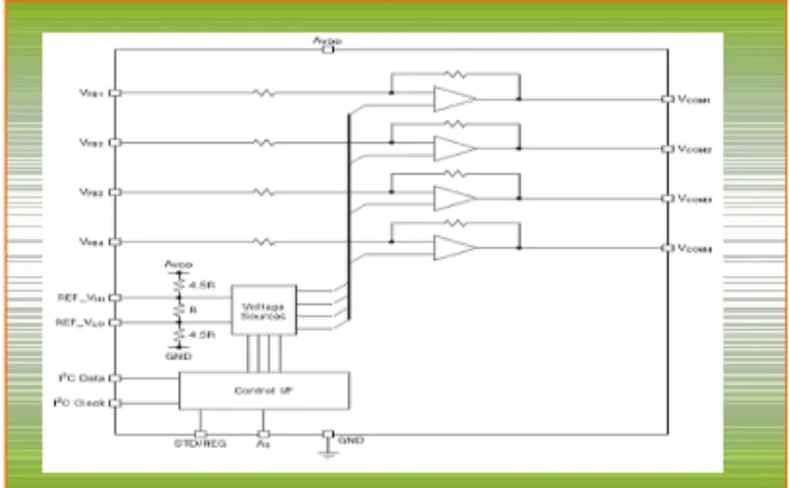
Fig. 6. The block diagram of the proposed potentiometer.
Fig. 6 shows the proposed potentiometer which consisted of digital signal input, voltage source and controller.
The OLED panel input voltage range is 12~18V.
Input voltage means battery voltage(3.3V). Output voltage means input voltage of PM OLED panel.
Basic voltage regulator scheme is not only voltage divider(analog method) but digital potentiometer(digital method). Switching frequency 1.2MHz containing 1.5A, 36V switch.
Ⅵ. Experiment Results
Fig. 7 shows the proposed PM OLED dc-dc converter. It is connected to the PM OLED panel.
The prototype dc-dc converter voltage range is 12V, 14V, 18V.
Fig. 7. The multi-channel dc-dc converter prototype for PM OLED.
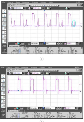
Fig. 8(a) shows the waveform used for typical voltage divider dc-dc converter. Fig. 8(b) presents the waveform multi-channel method.
(a)
(b)
Fig. 8. The multi-channel dc-dc converter prototype for PM OLED.
As shown Fig. 5, compared with general PM OLED dc-dc converter that performance complete voltage regulating, this system remove the FFN(Frame Frequency Noise).
Fig. 9 shows the curve of efficiency between conventional converter and the proposed converter with respect to load condition. The maximum efficiency of conventional dc-dc converter is around 82%. But the efficiency of the proposed dc-dc converter is almost 85% under wide load range.
Fig. 9. Comparison of the efficiency between conventional converter and the
proposed converter.
Ⅴ. Conclusions
In this study, I proposed an efficient PM OLED multi-channel dc-dc converter with digital control method using potentiometer.
As a result, we can get a 84.5% at 18V, 180mA in present state using digital voltage control method.
And, this system remove the FFN(Frame Frequency Noise). Moreover, we can use this method, we can obtain the COF(chip on FPC) area 1.5×1.5[cm]. It is clearly has a reduce level of 40% comparing 1.5×2.5[cm].
References
[1] C. W. Tang. S. A. Vanslyke, Appl. Phys. Lett.
51(1987)913.
Burns, A. B. Holms, Nature 347(1990)539.
[3] Sung-Joon Park, Ok-Tae Kim and Hee-Je Kim,
"Electrode Thickness Optimization at Full Color OLED and Anaysis of Power Comsumption", KIEE International Transactions on EA, vol. 4-C, No. 3, pp 106-110, 2004 [4] H. Kubota, S. Miyaguchi, S. Ishizuka, T.
Wakimoto, J. Funaki, Y. Fukuda, T. Watanabe, H. Ochi, T. Sakamoto, T. Miyake, M. Tsichida, I. Ohshita, T. Tohma., "Organic LED full color passive-matrix display", Journal of Luminescence, 87-89, pp 56-60, 2000
[5] Christophe Py, Marie D'Iorio, Ye Tao, John Stapledon, Paul Marshall, "A Passive matrix addressed organic electroluminescent display using a stack of insulators as row separators", Synthetic Metal, vol 113, pp 155-159, 2000
BIOGRAPHY
Sung-Joon Park (Member)
2000 : BS degree in Electrical Engineering, Dongui University.
2002 : MS degree in Electrical Engineering, Pusan National University.
2009 : Ph. D degree in Electrical Engineering, Pusan National University.
2002~2003 : Research Engineer, LG Electronics Institute of Technology.
2004~Present : Korea Hydro-Nuclear Power Company.