A Novel Negative-Output High Step-up Ratio DC-DC Converter Based on Switched-Inductor Cell
Ho-Yeon Kim
*, Eun-A Moon
*, Minh-Khai Nguyen
**★Abstract
A high boost dc-dc converter based on the switched-inductor cell (SL-cell) is suggested in this paper. The suggested converter can provide a high voltage gain that is more than 6. Moreover, the voltage gain can be easily increased by extending a SL cell or a modular voltage boost stage. This paper shows the key waveforms, the operating principles at the continuous conduction mode (CCM), and a comparison between the suggested converter and the other non-isolated converters. In addition, the extension of the suggested converter is presented. The simulation results were shown to reconfirm the theoretical analysis.
Key words:non-isolated dc-dc converter; high-voltage gain; switched-inductor; boost converter; continuous conduction mode
* Graduate School, Chosun University, Gwangju, Korea
** Dept. of Electrical and Electronics Engineering, Ho Chi Minh City University of Technology and Education, Ho Chi Minh City, Viet Nam
★ Corresponding author
E-mail:[email protected], Tel:+84-8-3896 1333
Manuscript received Feb. 24, 2019; revised Mar. 7, 2019; accepted Mar. 28, 2019.
This is an Open-Access article distributed under the terms of the Creative Commons Attribution Non-Commercial License (http://creativecommons.org/licenses/by-nc/3.0) which permits unrestricted non-commercial use, distribution, and reproduction in any medium, provided the original work is properly cited.
I. Introduction
Nowadays, we are facing pressure from environment protection and global surface temperature. The energy sources are depleting, hence the development of renewable energy is the most-effective solution.
However, the available renewable energies such as wind power, solar cells, and fuel cells are dependent on the weather conditions, and their output voltages are low and instability. Thus, a high boost voltage conversion should be used to convert a low voltage to a high voltage for grid-connected inverter. The functional block diagram of the power-conversion system is shown in Fig. 1. A high boost dc-dc converter is used to convert a low voltage into a high voltage dc bus [1].
DC-DC Converter Low Voltage
Side
High Voltage Side Fig. 1. Functional diagram of power-conversion system.
Many high boost dc-dc converters have been researched and obtained a high-voltage gain in both isolated and non-isolated topologies. For the isolated topologies [2][3], a high-frequency transformer is used to isolate the input and the output with a two-stage dc-ac-dc power conversion. The converter circuit’s size and cost are increased. Moreover, the leakage inductances can be caused a voltage spike on switches. Owing to these limitations, the transformer-based topologies cannot achieve a high efficiency as non-isolated topologies. For the non-isolated topologies, many high boost dc-dc converters have been proposed in [4-15].
273
S
2C
1C
0V
iS
1D
1D
0R L
2L
1(a)
S
2C
1C
0V
iL
S
1D
1D
2D
0R L
1(b)
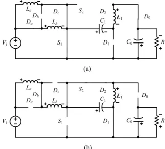
Fig. 2. Voltage-lift technique based non- isolated dc-dc converter in (a) [14] and (b) [15].
The high boost converters with coupled-inductor are proposed in [4][5] can obtain the high voltage gain; however, the leakage inductance of the coupled inductor causes high voltage spike on switches. The non-coupled-inductor converters can achieve a high-voltage gain with a high efficiency because of lacking the leakage inductance. Different structure and techniques including cascaded [6], switched-inductor [7], switched-capacitor [8], interleaved [9][10], and voltage-lift [11-15] techniques have been introduced. In switched-capacitor technique [8], by combining several switches and capacitors with minimum inductor achieving a higher output voltage can be obtained. However, this technique uses a large of number of switches and capacitors, which increase the current stress of switching. In [12], series and parallel combinations of converters have been verified to improve the voltage gain of the converter. However, they can increase size, cost, and complexity of control.
Thus, it was not very interesting to researchers.
Moreover, the voltage lift techniques based on inductor and capacitor elements was proposed in [13][14] to decrease the voltage stress of switch, as shown in Fig. 2. The voltage lift technique can use for the applications with high efficiency, simple structure, and cheapness when compared with other techniques. In addition, the lack of additional switches that lead to the complexity of the control system of a dc–dc converter is an important feature of this technique. The non- isolated dc–dc boost converters using the voltage technique has been presented in [15] with the higher voltage gain. In this topology, the output voltage of the proposed converter is negative with respect to input ground. However, the voltage gain is not high.
This paper presents a dc-dc converter based on switched-inductor technique with high-boost conversion ratio. The following characteristics of the proposed converter are: easy to increase the voltage gain, high-boost voltage gain, and using the small duty cycle. The content of the paper is
organized as follows. In Section II, the suggested topology is presented along with the circuit operation principle and steady-state analysis in continuous conduction mode (CCM). Some comparisons with other converters are shown in Section III.
The design procedure along with the simulation results in PLECs software is given in Section IV.
Finally, some conclusions are discussed on Section V.
Ⅱ. Proposed Converter
Fig. 3 shows the suggested dc-dc converter. It consists of one SL cell (L
a, L
b, D
a, D
b, and D
c), two power switches (S
1-S
2), modular voltage boost stage (L
1, D
1, D
2, and C
1), one diode (D
0), one capacitors (C
o), and a resistive load (R). Fig.
4 shows the key waveforms of the suggested
converter operating in the CCM. The operation
of switches is controlled by the PWM technique
and opposes each other. The switches, S
1and S
2,
are turned on and off alternately. To simplify the
circuit analyses of the suggested converter in the
CCM, the following assumptions were made: 1) all
devices are ideal and lossless; 2) the capacitance
of the capacitors is large enough to maintain the constant capacitor voltage; and 3) the current flow to the inductor increases or decreases linearly.
La S2
Da C1
C0
Vi
Dc Lb
S1
Db
D1
D2
D0
R L1
SL cell MV-Boost Stage
Fig. 3. Proposed dc-dc converter.
S1
S2
T
t t
t ILa=ILb
∆ILa Ton
t IL1
∆IL
Toff
Fig. 4. Key waveforms of the suggested converter.
La S2
Da C1
C0 Vi
Dc Lb
S1
Db
D1
D2
D0
R L1
La S2
Da C1
C0
Vi
Dc
Lb
S1
Db
D1 D2
D0
R L1
(a)
(b)
Fig. 5. Operating modes of the suggested converter:
(a) state 1 and (b) state 2.
A. Converter Analysis in CCM
Fig. 4 shows the key waveforms of the suggested converter in the CCM. Fig. 5 shows the operating state of the suggested converter.
State 1-[0 ≤ t ≤ DT, Fig. 5(a)]: S
1is turned
“ON”. The L
aand L
binductors are charged. The D
a, D
cdiodes are forward-biased, while the D
bdiode is reverse-biased. The D
0diode is forward-biased and D
1is reverse-biased. The time interval in this mode is T
on= DT, where D and T are the duty cycle of switch S
1and the switching period, respectively.
1
1 1
.
La Lb
a b i
L
C o
di di
L L V
dt dt
L di V V
dt
ì = =
ïï í
ï = -
ïî
(1)
State 2-[ DT < t ≤ T, Fig. 5(b)]: S
1is switched “OFF” and S
2is switched “ON”; the D
0diode is reverse-biased while the D
1diode is forward-biased. The time interval in this mode is T
off= (1-D)ㆍT. During this mode, the L
aand L
binductors are discharged, while the L
1capacitor is charged. The following formulas are derived as
1
1 1 1
.
La Lb
a b i C
L C
di di
L L V V
dt dt
L di V dt
ì + = -
ïï í
ï =
ïî
(2)
Through the application of the volt-second balance law to the inductors L
a, L
b, and L
1in a steady state, (1) to (2) yield the following equations:
( ) ( )
( )
( ) ( )
1 _off
_off
1 1
1 0
1 0
1 0,
i i C Lb
i Lb
C o C
DV D V V V
DV D V
D V V D V
ì + - - - =
ïï + - =
í ï - + - =
ïî
(3)
By substituting (3) into (1), the capacitor C
1voltage and output voltage of the suggested converter are as follows:
( )
1
1 1
1 ,
1
C i
o i
V DV
D
V D V
D D
ì = +
ï -
ïí +
ï = ïî -
(4)
B. Extension of the Suggested Converter
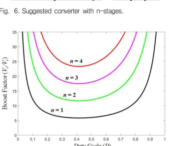
According to Fig. 6, the suggested converter
is possible to verify an n-stage boost converter by adding the modular voltage boost stage (one inductor, one capacitor and two diodes). The voltage gain with n from 1 to 4 is shown in Fig.
7. The extension with n-stage boost structure, the SL-cell and two switches are kept in the power circuit, and (n + 1) inductors, (n + 1) capacitors, and (2n + 1) diodes are used for modular voltage boost stage.
La S2
Da C1
C0
Vi
Dc
Lb
S1
Db
D1
D2
D0
R L1
SL cell Stage 1 Cn
Dn
Dn+1
Ln
Stage n
Fig. 6. Suggested converter with n-stages.
Fig. 7. Voltage gain comparison.
For analysis, S
1is ON and S
2is OFF, D
0is conducted, and D
1, D
2, …, D
nare Off. Moreover, L
2, L
3, …, L
n+1and C
1, C
2, …, C
nare in series connection. The series connection of n-capacitors increases V
o. When S
1is OFF and S
2is OFF, and D
1, D
2, …, D
nare directly biased and D
0is reversely biased. The voltage gain of the n-stage converter in CCM is given
( )
( 1 1 )
o i
n D
V V
D D
= +
- (5)
Ⅲ. Comparison with Other Non-Isolated High-Boost Converters
The comparison between the suggested converter and other non-isolated high-boost dc-dc converters is shown in Table 1. When compared with the non-isolated dc-dc converters in [13]-[15], the suggested converter uses one more inductor and diodes. Moreover, the suggested converter has less one switch and one capacitor than the non-isolated converter in [14]. Although, the suggested converter uses more components, the suggested converter can save the size of the inductor in SL cell and has higher voltage gain.
Fig. 8 shows a comparison between the voltage gains of the non-isolated high boost dc-dc converters in the CCM. As shown in Fig. 8, the voltage gain of the proposed converter is the highest at the same duty cycle.
Table 1. Comparison between the suggested converter and other high boost dc-dc converters.
Switch Inductor Capacitor Diode Voltage gain Converter
in [13] 2 2 2 2
D(
11-D)
Converter
in [14] 3 1 3 2 ( )
1 2
1 D D D D - +
-
Converter
in [15] 2 2 2 3
D(
11-D)
Suggested
converter 2 3 2 6
1(
1)
D
D D
+ -
![Fig. 2. Voltage-lift technique based non- isolated dc-dc converter in (a) [14] and (b) [15].](https://thumb-ap.123doks.com/thumbv2/123dokinfo/5623676.499885/2.892.473.795.142.508/fig-voltage-lift-technique-based-non-isolated-converter.webp)