415 Journal of International Conference on Electrical Machines and Systems vol. 3, no. 4, pp. 415~421, 2014
Development of High Efficiency Boost DC/DC Converter For EV
Sung-Geon Song*, Sang-Hun Lee**, Hyun-Jig Song**, and Seong-Mi Park***
Abstract
– In this paper, reactorless high efficiency boost DC/DC converter for EV isproposed. In proposed converter, improves efficiency because decrease power loss when the switches are turned on/off using zero current switching (ZCS) at all switch of primary full bridge. By replacing reactance ingredients of L-C resonance circuit for ZCS with leakage inductance ingredients of high frequency transformer, it reduces system size and expense because of not add special reactor. For validity verification of proposed converter, in the paper implements simulation using PSIM and perform experiment by making 5KW DC/DC converter. In experimental results, efficiency of proposed converter conformed superiority.
Keywords:
DC/DC converter, ZCS, Full-bridge, EV, Resonant circuit1. Introduction
Today the use of electricity is increasing with the development of industries and vehicles with internal combustion engine are rapidly increasing for convenience of travel. To produce electricity and drive internal combustion engines, fossil fuels must be used, causing serious environmental problems. These days many people are making efforts to reduce CO2 which is the main culprit for the destruction of global environment. In particular, as vehicles account for over 50% of the CO2 emissions, active efforts to reduce them are being made all over the world. Typical examples of such efforts are the improvement of fuel economy and the introduction of electric vehicles. Recently, hybrid vehicles that use both internal combustion engine and electric motor have been developed with effective improvement of fuel economy. It is expected that in the future, the percentage of vehicles using internal combustion engine will gradually decrease and ultimately be replaced with pure electric vehicles and fuel-cell vehicles[1][2]. As the use of electric motors is increasing, traction motors mainly use 300 V or higher voltages considering losses and advantages in motor design. However, since such high-voltage power supply systems have such problems as electric shock, systems like NEV (Neighborhood Electric Vehicle) use low voltage batteries of maximum 70 V. Due to safety and efficiency issues, batteries are using low voltage while
motors use high voltages. Thus, it is essential to develop a boost DC/DC converter with at least 4-fold boosting efficiency[3][4]. Furthermore, an insulation-type converter needs to be developed to address the electric safety issue.
Accordingly, this paper proposes an insulated DC/DC converter that uses a voltage multiplier circuit composed of diodes and condensers at the output for high voltage multiplication, in particular, a new insulation-type DC/DC converter with a serial connection of two voltage multiplier circuits for 4-fold boosting. The proposed method maintained the ratio of the transformer as 1:1 for identical input and output characteristics of the converter considering the regenerative braking of vehicles in the future. Furthermore, the proposed converter reduced the switching loss of the power switch using a serial L-C resonance, and the size and cost of the total system can be reduced by replacing the reactance component required for the L-C resonance circuit with a transformer leakage reactance[5] .
To verify the feasibility of the proposed insulated DC/DC converter using a voltage multiplier circuit, a simulation was conducted using PSIM, and the real converter was fabricated and tested. It was found that up to 4-fold boosting was possible with the voltage multiplier circuit and a serial circuit only with no separate control, and the maximum efficiency of the converter was very high at around 97%.
2. Theories Power Converter for Electric Vehicle
Fig. 1 shows the block diagram of the proposed system which consists of two independent insulated DC/DC converters. The first converter is connected parallel to the battery and the output is connected serially with the battery. Thus, 2-fold boosting is possible by default.
* Digital Convergence Research Center, KETI, Korea ([email protected])
** Dept. of Automatic Electrical Engineering, Youngnam University College, Korea. ([email protected])
*** Dept. of Mechatronics, Korea Lift College, Korea. ([email protected])
Fig. 2 illustrates one insulated converter structure which uses high-frequency transformers for primary and secondary insulations. At the secondary side, a voltage multiplier circuit was configured with diodes and condensers. This proposed insulated DC/DC converter can perform 4-fold boosting through the voltage multiplier circuit and the serial connection at the secondary side. Therefore, the transformation ratio of the high-frequency transformer can be maintained at 1:1. / isolation DC DC converter / isolation DC DC converter battery inverter
Fig. 1. Proposed System Block Diagram
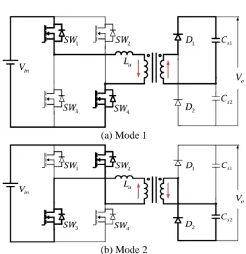
in V 1 SW SW2 3 SW 1 D 2 D o V a L 1 s C 2 s C 4 SW
Fig. 2. Proposed DC/DC Converter System Block Diagram Furthermore, to improve efficiency and reduce harmonic noise, a zero-current switching using L-C resonance must be used. For this purpose, this transformer used the leakage reactance of the insulating transformer and the condenser of the voltage multiplier circuit. Thus no additional reactor and condenser for resonance are needed, making the structure simpler and saving additional cost. The proposed insulated DC/DC converter can maintain the transformation ratio of the harmonic transformer at 1:1. Therefore, if bi-directional power exchange is considered in the future, as the characteristic impedances from the primary and secondary sides are identical, the dynamic characteristics of the power exchange are excellent and zero-current switching using resonance for switches of all directions of battery charging and discharging. in V 1 SW SW2 3 SW 1 D 2 D o V a L 1 s C 2 s C 4 SW (a) Mode 1 in V 1 SW SW2 3 SW 1 D 2 D o V a L 1 s C 2 s C 4 SW (b) Mode 2
Fig. 3. Proposed DC/DC Converter Operation Mode Fig. 3 shows the operation mode transition of the proposed DC/DC converter under no load and the operation principle is described below.
In Mode 1, SW1 and SW4 are turned ON and the input current is delivered to the secondary side through SW1 and SW4 and the high-frequency transformer when SW2 and SW3 are turned OFF. Furthermore, when the diode D1 is excited and Cs1 is charged from the input power, the charge current becomes serial resonance through La and Cs1 and supplies the input power to the load. Likewise, in Mode 2, SW2 and SW3 are turned ON and SW1 and SW4 are turned OFF. The input power is delivered to the secondary side through SW2 and SW3 and the high-frequency transformer. Furthermore, when the diode D2 is excited and Cs2 is charged from the input power, the charge current becomes serial resonance through La and Cs2 and supplies input power to the load just as in Mode 1. In this case, the current waveform which became serial resonance in Mode 1 and Mode 2 is sinusoidal waveform and can reduce switching loss as well as the surge that occurs during switching.
The SW1 and SW1 pair and the SW1 and SW1 pair are alternately turned ON and OFF, and the output power becomes twice the input power by the voltage multiplier circuit that combines diodes and condensers.
3. Principle of ZCS Resonance
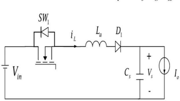
Fig. 4 is the equivalent circuit of Mode 1 in Figure in which the leakage inductance element La and the resonance capacitor element Cs1 of the secondary side have been reduced to the primary side of the transformer.
+
-aL
D
1 Li
1SW
inV
C
s VsI
oFig. 4. LC Serial Resonance Equivalent Circuit Assuming that the high-frequency transformer is ideal, the values are as follows:
(1) (2) The voltage and current of the equalized circuit of equations (1) and (2) can be expressed as follows:
(3) (4) However, the initial conditions are and
( ) =
Mode 1 : When the leakage inductance switch La turns on when , and La and Cs starts resonance. With the equations (3) and (4) and the initial conditions, the leakage inductance current during resonance can be expressed as follows:
(5) where L i 1 sw V s V o T T1 T2
Fig. 5. LC Experimental Waveforms Of Proposed DC/DC converter
As shown by the above equation, the resonance frequency is determined by inductor and condenser, and the condenser capacity must be able to handle the load current. The solutions of the above equations are shown below.
(6) (7)
where (Characteristic Impedance)
The resonance frequency calculated from the above equations is as follows:.
(8) Since Mode 1 finishes at a half of the resonance cycle, if the resonance frequency is greater than the switching frequency, the current flowing through the inductor becomes discontinuous. The inductor value that meets this condition is as follows:
(9) Mode 2 : The resonance finishes when , and the resonance capacitor is discharged by current , and the resonance capacitor voltage decreases. This voltage relational equation is as follows:
(10)
4. Measurement Results
In this section, To verify the feasibility of the proposed DC/DC converter, a simulation circuit using PSIM was configured as shown in Fig. 6. As mentioned in Introduction, the secondary voltage multiplier circuits were serially connected so that the output voltage will be four times the input voltage. The transformation ratio was set to 1:1 and the leakage inductance element was separately designated. The circuit constant equation used for PSIM simulation is shown in Table 1.
As shown in Fig. 7, when the switch SW1 was turned OFF, the current flowing in the leakage inductance became zero, thus fulfilling the ZCS (Zero Current Switching). Furthermore, the average voltage applied to each side of the resonance capacitor was 72V and the total average output was 4 times the input voltage, or 288V.
Fig. 6. Simulation Circuit Using PSIM Table 1. Simulation Parameters
Input Voltage Vin 72[V]
Output Voltage Vo 288[V]
Input Capacitor 100[uF]
Resonance Capacitor 7.5[uF]
Leakage Inductance 2[uH]
Switching Frequency 40[kHz] Resonance Frequency 41.093[kHz]
Load Resistance 100[Ω]
Transformation Ratio 1:1
Furthermore, the capacitor voltage applied to each voltage multiplier circuit by the alternate switching signals in Fig. 8 formed charge and discharge ripple voltages around the average voltage of 72V.
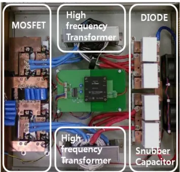
Fig. 9 shows the structure of the proposed DC/DC converter which was applied to the experiment for feasibility test.
(a) Swtich Voltage
(b) Leakage Voltage
(c) Capacitor Voltage
(d) Output Voltage
Fig. 7. Simulation Experimental Waveforms Using PSIM
1 Voltage S C 3 Voltage S C 2 Voltage S C 4 Voltage S C
Fig. 8. Simulation Capacitors Waveforms Using PSIM
Fig. 9. Photograph Of Proposed DC/DC Converter For the PWM controller, UC3825 from Texas Instrument was used, and for the primary MOSFET, and IXFN360N10T from IXYS was used for the secondary rectification diode to increase the capacities of current and voltage for boosting. The circuit constants used for this experiment are shown in Table 2.
Table 2. Experiment Parameters
Input Voltage Vin 72[V]
Output Voltage Vo 288[V]
Input Capacitor 100[uF]
Resonance Capacitor 5[uF]
Leakage Inductance 2[uH]
Switching Frequency 50[kHz]
Load Resistance 50.329[kHz]
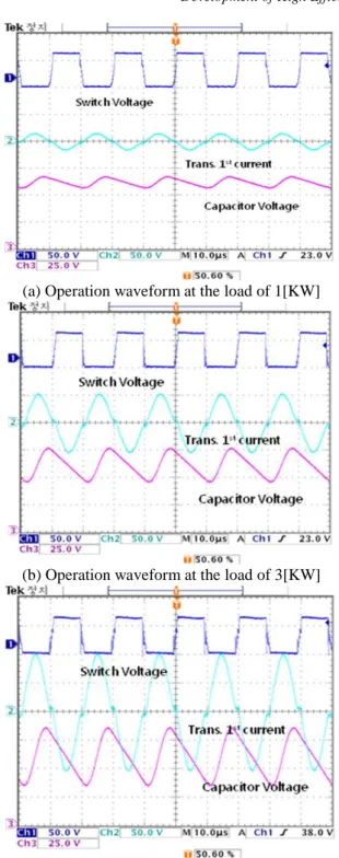
(a) Operation waveform at the load of 1[KW]
(b) Operation waveform at the load of 3[KW]
(c) Operation waveform at the load of 5[KW] Fig. 10. Operational Waveforms Of ZCS DC/DC Converter
Fig. 10 shows the voltage waveform applied to each load of the DC/DC converter and the current waveform of the primary transformer that has a leakage inductance, and the voltage waveform of the capacitor. Due to the alternate switching signals, the current waveform of the first side of the transformer becomes a sinusoidal graph. The results of the actual experiment using 5KW DC-DC converter showed soft switching by ZCS in all areas just like the simulation results, Fig. 11 shows the voltage waveforms of the four resonance capacitors. It can be seen that ripple voltage was
generated by the charging and discharging of all capacitors. The final output voltage is expressed as the sum of each capacitor voltage. Fig. 12 shows the voltages on the switch and the transformer input currents at 200 W and 1 KW. It shows that there is a current with a certain angle in addition to the sinusoidal waveform in the transformer input current by the exciting inductance of the transformer.
Fig. 11. Capacitors Voltage Waveforms Of DC/DC Converter
(a) SW1 voltage and current waveforms under the load of 200W
(b) SW1 voltage and current waveforms under the load of 10Kg
However, the current by this exciting inductance is unrelated to load, and its effect becomes smaller as the load increases. Fig. 13 shows a picture of the experiment with the proposed DC/DC converter connected with a variable resistance. The input and output voltages and currents at 5 KW are shown in
Fig. 13. Photograph of DC/DC Converter Linking Experiment
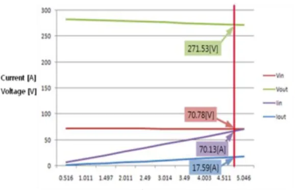
Fig. 14 At 5KW, the input voltage 70.76 V is boosted 4-fold to the output voltage 271.38 V.
Fig. 14. Experimental Waveforms Of Proposed DC/DC Converter
Fig. 15. Efficiency Of Output Power Comparison Fig. 15 shows the measurements of the converter's efficiency against the load. The highest efficiency was 96.967% at 2 KW, and the Euro efficiency was also very good at 96.103 %.
5. Conclusion
This This paper proposed a 5W high-efficiency insulated boost DC/DC converter for driving electric vehicles. The proposed method minimized the switch transient loss by soft switching with ZCS. Furthermore, its structure is simple because the reactor and capacitor for L-C resonance were replaced with the leakage reactor of an insulated transformer and the capacitor of a voltage multiplier circuit. A simulation was conducted using PSIM for theoretical design of the proposed converter and an actual 5KW converter was fabricated to test the feasibility of the proposed converter. The experiment with this converter found that soft switching by ZCS was possible and the converter worked stably in the entire range of load. The efficiency measurement showed very good efficiency with the highest efficiency of approximately 97% and the Euro efficiency of approximately 96 %. Based on these experiment results, the proposed insulated high efficiency boost converter could be used for the development of power conversion technology through miniaturization and light weight design.
References
[1] Toyota Environmental Technology Report "Toyota Hybrid System THS II"
[2] I.A. Khan, "DC-to-DC Converters for Electric and Hybrid Vehicles", Power Electronics in Transportation, 20-22, pp. 113-122, 1994, Oct.
Sung Geun Song was born in Gwang-Ju, Korea. He received the B.S., M.S. and Ph.D degrees in electrical engineering from Chonnam National University, in 1998, 2000 and 2007, respectively. From 2001 to 2004, he was a Research Scientist at PROCOM system, Ltd., From 2004 to 2005, he was a Research Scientist at SEO ELECTRONICS CO., LTD. Since 2008, he is working in KETI(Korea Electronics Technology Institute), where he is currently Gwang-Ju Regional Headquarter. His fields of interest are power electronics, motor drives, digital signal processing, tractions, and their control system
Sang-Hun Lee was born in Busan, Korea, in 1974. He received his B.S and M.S. degrees in Electrical Engineering from KyungSung University, Busan, Korea, in 2000, 2002, respectively. He received his Ph.D degrees in Mechatronics Engineering from Pusan National University, Busan, Korea, in 2006. He worked a Junior Researcher of Technology& Researcher at KTE, from 2002 to 2004, He has been with Kyungsung University, Busan, Korea, as a Researcher in the Advanced Electric Machinery & Electronics Center since 2006. Since 2014, he has been a Assistant Professor with the Department of Electrical Automatic Engineering, Yeungnam College of Science & Technology, Daegu, Korea. His major research field is Electrical Motor Drive with Power Electronics.
Hyun Jig Song was born in Deagu, Korea, in 1968. He received the B.S., M.S. and Ph.D degrees in electrical engineering from Yeungnam University, in 1991, 1993 and 1997, respectively. Since 2006, He has been an Associate Professor with the Department of Electrical Automatic Engineering, Yeungnam College of Science & Technology, Daegu, Korea. His current research interests include High-voltage Engineering, Electric power system and power electronics.
Seong-Mi Park received her B.S., M.S., and Ph.D. in Electronics and Computer Engineering from Chonnam National University, Gwangju, Korea, in 1986, 2001 and 2011, respectively. From 2004 to 2006, she was a Visiting Professor with the Department of Computer Engineering, Chonnam National University. Since 2013, she has been an Assistant Professor with the Department of Mechatronics Engineering, Korea Lift College, Geochang, Korea. Her current research interests include motor control, mechatronics and micro-machine automation.