광화학증착법에 의한 직접패턴 비정질 TiO
x
박막의 제조 및 저항변화 특성황윤경·이우영·이세진·이홍섭†
강원대학교 재료공학과
Resistive Switching Characteristic of Direct-patternable Amorphous TiO x Film by Photochemical Metal-organic Deposition
Yun-Kyeong Hwang, Woo-Young Lee, Se-Jin Lee, and Hong-Sub Lee†
Department of Materials Science and Engineering, Kangwon National University,
1, Kangwondaehak-gil, Chuncheon-si, Gangwon-do 24341, Korea (Received November 6, 2019: Corrected March 5, 2020: Accepted March 6, 2020)
초 록: 광화학증착법 (PMOD; photochemical metal-organic deposition)을 이용하여 photoresist 및 etching 공정없이 pattern 된 TiO
xresistive switching (RS) 소자를 제작 및 그 특성을 평가하였다. Ti(IV) 2-ethylhexanoate를 출발물질로 사 용하였으며 UV 노출시간 10 min에 광화학반응이 완료됨을 FTIR 분석을 통하여 확인하였다. 200
oC 이하 저온공정에서 직접패턴 된 20 nm 두께의 비정질 TiO
x박막의 균일한 두께의 패턴형성을 Atomic Force Microscopy를 통하여 확인하 였다. 별도의 상형성을 위한 후 열처리 공정 없이 4 μm 선폭의 전극위에 형성된 20 nm 두께의 비정질 TiO
xRS 소자는 4V 동작전압에서 on/off ratio 20의 forming-less RS 특성을 나타내었다. Electrochemical migration에 영향을 미치는 grain boundary 가 없어 소자간 신뢰성 향상이 기대되며, flexible 기판 또는 저온공정이 요구되는 메모리 소자 공정에서 PMOD 공정이 응용될 수 있음을 보여준다. Selector를 이용하여 crossbar array 구조를 도입할 경우 매우 간단한 구조의 저비용 메모리 소자를 구현할 수 있을 것으로 기대 된다.
Abstract: This study demonstrates direct-patternable amorphous TiO
xresistive switching (RS) device and the fabrication method using photochemical metal-organic deposition (PMOD). For making photosensitive stock solutions, Ti(IV) 2- ethylhexanoate was used as starting precursor. Photochemical reaction by UV exposure was observed and analyzed by Fourier transform infrared spectroscopy and the reaction was completed within 10 minutes. Uniformly formed 20 nm thick amorphous TiO
xfilm was confirmed by atomic force microscopy. Amorphous TiO
xRS device, formed as 6 x 6 μm square on 4 μm width electrode, showed forming-less RS behavior in ±4 V and on/off ratio ≈ 20 at 0.1 V. This result shows PMOD process could be applied for low temperature processed ReRAM device and/or low cost, flexible memory device.
Keywords: Resistive RAM, PMOD, resistive switching, non-volatile memory, patterning process
1. 서 론
Resistive RAM (ReRAM)은 차세대 비휘발 메모리 ferroelectric random access memory (FeRAM), ferroelectric field effect transistor memory (FeFET memory), phase change RAM (PCRAM), spin-toque transfer magnetic RAM (STT-MRAM), resistive RAM (ReRAM) 중 하나로 기존의 charge trap 방식의 아닌 재료의 상태 변화를 이용하는 메 모리를 말한다.1-8) ReRAM은 전이금속 산화물에서 관찰 되는 resistive switching (RS) 특성을 이용하는 메모리 소
자로 산소 이온의 electrochemical migration에 의해 그 RS 특성이 나타난다. 간단한 metal/insulator/metal (MIM) 구 조로 crossbar array 구조에 적용할 경우 저비용으로 높은 집적도의 메모리를 구현할 수 있어 많은 연구가 진행되 어 왔으나, ion migration RS 메커니즘으로 인하여 신뢰성 확보에 어려움을 겪고 있으며 filament 형성에 필요한 초 기 forming process 또한 기술적 과제로 남아있다.8-11)
광화학증착법(PMOD; photochemical metal organic deposition)은 용액증착법(CSD; chemical solution deposition) 의 하나로 UV 노광에 의해 광화학반응이 가능한 금속유
†
Corresponding author
E-mail: [email protected]
© 2020, The Korean Microelectronics and Packaging Society
This is an Open-Access article distributed under the terms of the Creative Commons Attribution Non-Commercial License(http://creativecommons.org/
licenses/by-nc/3.0) which permits unrestricted non-commercial use, distribution, and reproduction in any medium, provided the original work is
properly cited.
기물(metal-organic precursor)을 출발원료로 사용하여 photoresist를 이용한 별도의 pattern 공정 및 etching 공정 없이 pattern 된 산화물 박막을 얻을 수 있는 공정이다.12-14) Fig. 1은 PMOD 공정의 모식도로 먼저 photochemical precursor를 유기용매에 용해한 용액을 제조 후 spin coating을 통하여 기판위에 박막을 형성한다. 이후 soft bake를 통하여 유기용매를 제거한 후 UV exposure를 통 하여 metal-organic precursor의 ligand를 분리하게 되며 이 과정에서 일부의 유기물은 가스형태로 휘발되고 일부 유 기물은 잔류하게 된다. 메탈 원소의 경우 대기중의 산소 와 결합하여 산화물이 형성되는데 UV exposure 후 유기 용매에 씻어내면 UV에 노출된 영역만 산화물로 남게 되 고 나머지 영역은 유기용매에 용해되어 제거된다. 이후 post bake를 통하여 패턴 된 박막 내의 잔류 유기물을 제 거하여 최종적으로 원하는 형태의 패턴 된 박막을 얻을 수 있다.
PMOD 공정은 별도의 etching 공정 없이 패턴 된 박막 을 얻을 수 있는 장점이 있지만 CSD 공정의 특성 상 박 막 형성 후 잔류 유기물의 존재와 dense한 박막을 얻기 어려운 단점으로 인하여 금속산화물의 주요 응용분야인 산화물 반도체 또는 유전 박막에 적용시 잔류 기공에 의 한 저항증가 또는 누설 전류로 인하여 PMOD 공정응용 에 어려움이 있다.12-14)하지만 전이금속산화물을 이용하 는 음이온 기반의 RS 소자의 경우 위의 잔류기공에 의한 저항증가 또는 잔류 유기물에 의한 누설전류 등이 문제 되지 않으며, 또한 저온공정을 통한 비정질 상태에서도 RS 특성을 얻을 수 있어 PMOD 공정이 매우 유용한 응 용분야이다. 따라서 본 연구에서는 균일한 forming-less RS 특성 구현을 위하여 비정질의 TiOx를 PMOD를 이용
하여 별도의 photoresist 패턴 및 etching 공정없이 저비용 으로 제작이 가능한 RS 소자를 제작, 그 특성을 평가하 였다.
2. 실험방법
Ti(IV) 2-ethylhexanoate를 Ti 출발물질로 사용하였고 용 매는 hexane을 사용하였다. Ti(IV) 2-ethylhexanoate를 hexane에 용해 후 1시간 동안 교반하여 5 mM 농도의 용 액을 제조하였다. 제조된 광감응성 Ti 용액을 Acetone, DI water, ethanol에서 각각 20s 동안 초음파로 세척된 SiO2 (300 nm)/ p-type Si 기판 위에 spin coater를 이용하여 3,500 rpm에서 25s, 5,000 rpm에서 35초간 스핀 코팅하였다. 이 후 100°C에 1분간 soft bake를 진행하였으며 원하는 두께 의 박막을 얻기 위하여 이 spin coating 공정을 두 번 반 복하였다. 이 후 mask aligner를 이용하여 contact mode로 UV (350W mercury arc lamp) 노광 공정을 실시하였다. 용 매로 사용된 hexane을 이용하여 develop 후 잔류 유기물 제거를 위하여 200°C에 2분간 post bake하였으며 최종적 으로 20 nm 두께의 비정질 TiOx 박막을 얻었다.
노출 시간에 따른 ligand 분해과정을 관찰하기 위하 여 적외선 흡수분광(FTIR: Fourier transform infrared spectroscopy, PerkinElmer Frontier FT-IR) 분석을 실시하 였으며, atomic force microscope (AFM, Park systems, XE- 100)를 이용하여 패턴 된 박막의 패턴 모양 및 두께를 확 인하였다. RS 특성 측정을 위하여 상 하부 전극으로 Au, Pt를 각각 사용하였으며 최종적으로 Au (40 nm)/TiOx (20 nm) / Pt (40 nm) 구조의 소자를 제작, Keithley 2636B SourceMeter를 이용하여 RS 특성을 평가하였다.
Fig. 1. Schematic diagram of the photochemical metal-organic deposition method.
3. 결과 및 고찰
Fig. 2(a)는 코팅된 Ti(IV) 2-ethylhexanoate 박막의 UV 노 출시간에 따른 1,000~3,500 cm−1 범위의 FT-IR 측정결과 이다. 2,959, 2,934, 2,871 cm−1파수에서 alkyl(−CH3) 그룹 과 alkene(−CH2) 그룹의 asymmetric (νa), symmetric (νs) stretching 진동모드에 의한 absorption peak이 각각 관찰 되었으며,12,15,16) 1,270~1,600 cm−1 영역에서는 C-O bond 의 symmetric stretching, C-O-H in-plane bending, CH2 out of plane wagging 진동모드에 의한 peak이 각각 관찰되었
다.12,15,16) 이들은 2-ethylhexanoate ligand로부터 기인하는
absorption peak으로 UV 노출시간의 증가에 따라 peak의 intensity가 감소함을 관찰할 수 있었다. 따라서 Fig. 2(a) 는 UV 노출에 의해 2-ethylhexanoate ligand가 분해됨을 보 여주며 10 min 노출 시 UV에 의한 ligand의 광분해반응 이 완료됨을 알 수 있다. Fig. 2(b)는 UV 노출 시 Ti(IV) 2- ethylhexanoate 분해를 나타내는 모식도로 2-ethylhexanoate ligand는 UV 노출 시 CO2와 C7H14 또는 C7H16으로 분해 되는데 CO2의 경우 gas 형태로 휘발되며 C7H14와 C7H16
는 post bake 공정에서 휘발된다. Ti metal 원소의 경우 대 기로부터 산화되어 TiOx 형태로 기판에 남게 된다.16)
Fig. 3(a)는 SiO2 기판 위에 10×10 µm 사각형 모양으로 패턴 된 비정질 TiOx박막의 AFM topography 측정 이미 지이며, Fig. 3(b)는 Fig. 3(a)의 red line과 green line의 height profile을 나타낸다. Spin coating을 2회 시행했을 때
~20 nm 두께의 박막이 형성되었음을 확인할 수 있었으며 edge 부분을 제외한 박막 내부 높이의 최대 최소 차이는
~4.5 nm로 비교적 균일한 두께의 박막을 얻을 수 있었다.
패턴 된 박막의 edge 부분의 높은 모양과 벽의 경사는 Near field diffraction에 의한 것으로 판단된다. Chrome mask를 통과하는 빛은 회절에 의해 퍼져나가게 되는데, 코팅된 precursor film 두께로 인한 기판과 마스크의 간극 으로 PMOD 박막은 photomask의 디자인 크기보다 커지 게 되며, 이로 인한 박막 상 하부의 면적의 차이 및 벽의 경사가 발생하게 된다.
PMOD로 패턴 된 비정질 TiOx 박막의 저항변화 특성 을 측정하기 위해 mask aligner를 이용하여 Fig. 4(a)와 같 이 4 µm 선폭으로 패턴 된 Pt (40 nm) 전극 위에 6×6 µm
Fig. 3. (a) AFM topography image of patterned TiO
xthin films on SiO
2/Si substrate and (b) height profiles (profile colors correspond to red and green line of topography image).
Fig. 2. (a) FTIR absorption spectrum of Ti(IV) 2-ethylhexanoate thin film according to UV exposure time (0, 3, 5, and 10 minutes).
(b) Schematic diagram of photochemical reaction by UV exposure.
로 패턴 된 20 nm 두께의 TiO2 소자를 제작하였다. 상부 전극으로는 Au (35 nm)를 사용하였으며 adhesion layer Ti 4 nm를 사용하였다. 최종적으로 Fig. 4(b)와 같은 형태의 단위 소자를 제작하였으며 I-V 특성을 평가하였다.
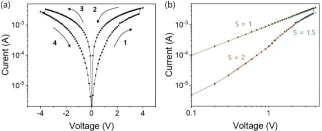
Fig. 5(a)는 소자에서 측정된 RS 특성을 나타낸다. 그림 안의 화살표는 스위칭 방향을 나타내며 + 전압에서 low resistance state (LRS) 스위칭, – 전압에서 high resistance state (HRS)를 나타내어 반시계 방향의 bipolar 스위칭 특 성을 보였다. 박막의 초기저항상태는 HRS였으며 동작전 압 ±4 V에서 별도의 forming process 없이 RS 특성이 관 찰되었으며 읽기전압 0.1 V에서 on/off ratio 20의 RS 특 성을 나타내었다.
±3.5 V 부근에서 갑작스러운 RS가 관찰되었으며 이 는 전형적인 filament type의 resistive switching curve로 TiOx 박막 내의 conducting filament의 형성, 산소공공의 electrochemical migration에 의한 conducting filament의 국부적인 소실, 회복에 의해 RS 특성이 나타남을 의미 한다.17-19)
Fig. 5(b)는 positive bias의 log-log plot으로 HRS curve의 경우 0 V~0.2 V 영역에서 slope ~1.1의 기울기가 관찰되
었으며, 0.2 V~2.2 V 영역에서는 slope ~2, 2.2 V~3.7 V 영 역에서 slope ~1.5 나타내었다. 전압이 증가함에 따라 Ohmic → space charge limited current (SCLC) 거동을 보 이다 다시 Ohmic에 가까워지는 거동을 보였다. 이는 Joule heating에 의해 thermally activated carrier의 증가로인한 거 동으로 보인다.20) 반면 LRS의 경우 박막내의 conducting filament 형성으로 인하여 0 V~4 V 모든 전압영역에서 slope ~1의 Ohmic 거동을 보였다. RS 특성에서 보는 바 와 같이 PMOD 공정에서 자연산화된 TiOx 비정질 박막 은 상당히 높은 전류량을 나타내며, 이는 박막 형성 시 낮 은 산화수의 TiOx가 형성됨을 예상할 수 있다. 또한 Forming process 없이 filament type의 RS 거동을 나타내 는 원인으로는, 박막내부 낮은 저항의 TiOx와 공정 중 표 면 부에 국부적으로 형성되는 높은 산화수의 고 저항 영 역으로 인하여 초기상태에서 전압인가 시, 표면 국부영 역에 전압이 집중되어 forming을 동반하는 국부영역에서 의 저항변화가 나타나기 때문인 것으로 판단된다. 현재 의 transistor의 동작전류를 고려하였을 때 ReRAM 응용 을 위해서는 저 전류 동작이 요구되므로, 향후 동작전류 를 낮출 수 있는 방안이 필요할 것으로 판단되다.
Fig. 5. (a) Resistive switching characteristic of amorphous TiO
xfilm and (b) double logarithmic plot of positive bias.
Fig. 4. Optical microscope images of (a) 6 x 6 μm patterned TiO
xfilm on bottom electrode and (b) final MIM device after top electrode
deposition.
4. 결 론
본 연구에서는 차세대 비휘발 메모리 ReRAM에 응용 하고자 PMOD를 이용한 비정질 TiOx RS 소자를 제작, 특성평가를 수행하였다. 200oC 이하 저온공정을 통하여 형성된 20 nm 두께의 비정질 TiOx 박막은 비교적 균일 한 두께로 패턴형성이 되었으며 별도의 상형성을 위한 후 열처리 공정 없이 비정질 상태로 4 V 동작전압에서 on/off ratio 20의 resistive switching 특성을 나타내었다.
Electrochemical migration에 영향을 미치는 grain boundary 가 없어 소자간 신뢰성 향상이 기대되며, flexible 기판 또 는 저온공정이 요구되는 메모리 소자 공정에서 응용될 수 있을 것으로 판단된다. Selector를 이용하여 crossbar array 구조를 도입할 경우 매우 간단한 구조의 저비용 메모리 소자를 만들 수 있을 것으로 기대 된다.
감사의 글
This work was supported by the National Research Foundation of Korea (NRF) grant funded by the Korea government (MSIT) (2019R1F1A1059637) and a 2019 Research Grant from Kangwon National University.
References
1. O. Auciello, J. F. Scott, and R. Ramesh, “The Physics of Fer- roelectric Memories”, Phys. Today, 51(7), 22 (1998).
2. S. Mathews, R. Ramesh, T. Venkatesan, and J. Benedetto,
“Ferroelectric Field Effect Transistor Based on Epitaxial Per- ovskite Heterostructures”, Science, 276(5310), 238 (1997).
3. J. Lee, S. Choi, C. Lee, Y. Kang, and D. Kim, “GeSbTe depo- sition for the PRAM application”, Appl. Surf. Sci., 253(8), 3969 (2007).
4. Z. Li and S. Zhang, “Domain-wall dynamics driven by adi- abatic spin-transfer torques”, Phys. Rev. B, 70(2), 024417 (2004).
5. A. Sawa, “Resistive switching in transition metal oxides”, Mater. Today, 11(6), 28 (2008).
6. R. Waser, R. Dittmann, G. Staikov, and K. Szot, “Redox- Based Resistive Switching Memories-Nanoionic Mecha- nisms, Prospects, and Challenges”, Adv. Mater., 21(25-26), 2632 (2009).
7. H.-S. Lee, “The Latest Trends and Issues of Anion-based
Memristor”, J. Microelectron. Packag. Soc., 26(1), 1 (2019).
8. H.-Y. Kim, S.-J. Park, and G. E. Jang, “Microstructure and Electrical Properties of SrBi
2Ta
2O
9Ferroelectric Thin Films Prepared by RF Magnetron Sputtering Method”, J. Micro- electron. Packag. Soc., 6(2), 51 (1999).
9. A. Sawa, “Resistive switching in transition metal oxides”, Mater. Today, 11(6), 28 (2008).
10. B. J. Choi, D. S. Jeong, and S. K. Kim, “Resistive switching mechanism of TiO
2thin films grown by atomic-layer depo- sition”, J. Appl. Phys., 98(3), 033715 (2005).
11. H. S. Lee, S. G. Choi, H.-H. Park, and M. J. Rozenberg, “A new route to the Mott-Hubbard metal-insulator transition:
Strong correlations effects in Pr
0.7Ca
0.3MnO
3”, Sci. Rep., 3, 1704 (2013).
12. J.-S. Hwang, W.-S. Kim, H.-H. Park, and T.-S. Kim “Sol-gel Mechanism of Self-patternable PZT Film Starting from Alkoxides Precursors”, J. Korean Ceram. Soc., 40(4), 285 (2003).
13. H.-H. Park, S. Yoon, H.-H. Park, and R. H. Hill, “Electrical properties of PZT thin films by photochemical deposition”, Thin Solid Films, 447-448, 669 (2004).
14. C.-S. Hong, H.-H. Park, S.-J. Wang, J. H. Moon, H.-H. Park, and R. H. Hill, “Formation of photoresist-free patterned ZnO film containing nano-sized Ag by photochemical solution deposition”, Appl. Surf. Sci., 252(21), 7739 (2006).
15. W. J. Potts, and R. A. Nyquist, “Factors affecting the out-of- plane hydrogen deformation frequencies in olefins and their derivatives”, Spectrochim. Acta A, 15, 679 (1959).
16. H.-H. Park, H.-H. Park, and R. H. Hill, “Direct-patterning of SnO
2thin film by photochemical metal-organic deposition”, Sens. Actuators, A, Phys., 132(2), 429 (2006).
17. M.-J. Lee, C. B. Lee, D. Lee, S. R. Lee, M. Chang, J. H. Hur, Y.-B. Kim, C.-J. Kim, D. H. Seo, S. Seo, U.-I. Chung, I.-K.
Yoo, and K. Kim, “A fast, high-endurance and scalable non- volatile memory device made from asymmetric Ta
2O
5-x/TaO
2-x