P1-11 / Y.-J. Lee
IMID 2009 DIGEST •
Abstract
We attempted modulation of hydrogen dilution ratio to achieve both the minimal incubation layer and high deposition rate. The incubation layer thickness was estimated by transmission electron microscopy (TEM) and crystallization fraction was measured by Raman spectroscopy.
1. Introduction
The nanocrystalline silicon thin film transistor (nc-si TFT) was the current industrial standard in large area electronics. The nc-si film has superior stability and field effect mobility better than amorphous silicon films for applications to thin film transistor [1, 2]. The most fabrication of nc-si required additional process post annealing or high process temperature (≥600 ℃) [3, 4]. These process are increased fabrication time and cost. We attempted directly to deposit nc-si film at low temperatures (≤ 200℃) to use flexible substrates such as plastics. However the amorphous incubation layers formed at the onset of deposition [5]. This fact was known to deteriorate the performance of the transistors because bottom-gate TFT channel is formed in the lower part of active layers [6]. In order to have thin incubation layer at low temperature, we controlled the hydrogen dilution ratio (HDR) at catalytic chemical vapor deposition (Cat-CVD). Recently, the doped layer deposited by Cat-CVD has been widely used for device such as solar cell [7]. The TFT device is in need of phosphorous-doped silicon (P-doped si), n-type si films for ohmic contact between active layer and source/drain electrode. To fabrication of bottom-gate TFT without vacuum break, we investigated n-type si and SiNx films at low
temperature using Cat-CVD.
2. Experimental
The nc-si, n-type si and SiNx films were deposited
directly using Cat-CVD. The catalyst was tungsten wire of 0.4 mm diameter and the temperature of catalyst was 1740 ℃ by electrical power. The substrate temperature was lower 200 ℃. To obtain nc-si films, the source gas was mixture of silane (SiH4) and hydrogen (H2). We
attempted hydrogen dilution ratio (HDR) control for minimal incubation layer thickness. The HDR was calculated by following equation.
HDR = [H2]/ ([H2] + [SiH4]) × 100 % [1]
Where [H2] and [SiH4] are flow rates in standard
cubic centimeter per minute of H2 and SiH4,
respectively. The crystallization fraction of the nc-si film was measured by Raman spectroscopy and structure of the as-deposited film was studied with transmission electron spectroscopy (TEM). The n-type si films deposited on substrate with control the PH3/SiH4 mixing ratio from 1 % to 15 %. To obtain
SiNx, the NH3/SiH4 and H2/SiH4 mixing ratio were
controlled by regulation of NH3 and H2 flow rates.
The resistance and breakdown voltage determined with measurement of current-voltage (I-V) and capacitance-voltage (C-V).
3. Results and discussion
The Fig. 1(a) shows the dependence of the deposition rate on the HDR. When the HDR was increased from 50 % to 70 %, the deposition rate was reduced by 20 % and the Fig. 1(b) shows the
The Study of Nanocrystalline Silicon Bottom-gate Thin Film
Transistor Fabricated at Low Temperature for Flexible
Display
Youn-Jin Lee
1*, Kyoung-Min Lee
2, Jae-Dam Hwang
1, Kil-Sun No
1, Kap Soo
Yoon
3, Sung Hoon Yang
3and Wan-Shick Hong
1,21
Dept. of Nano Science and Technology, University of Seoul, Seoul 130-743, Korea
Phone:+82-2-2210-5718 , E-mail: [email protected] 2
Dept. of Nano Engineering, University of Seoul, Seoul 130-743, Korea
3
Samsung Electronics Co.,Ltd., Gyeonggi-Do 446-711, Korea
P1-11 / Y.-J. Lee
• IMID 2009 DIGEST
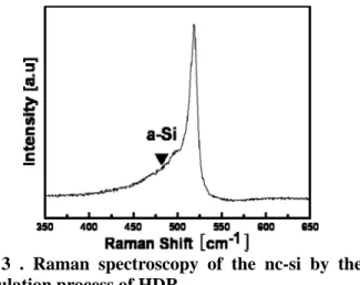
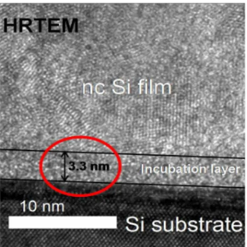
deposition rate was further reduced to one sixth of the initial value when the HDR was increased to 95 %. The incubation layer thickness is decreased as hydrogen dilution ratio increase. Therefore we developed modulation process and obtained minimal incubation layer thickness as well as high crystallization fraction and deposition rate. The change in HDR with time is shown in Fig. 2 first; the source gas of 95 % HDR was injected into the chamber for 10 minutes. The channel current is expected to flow within 10 nm from the bottom in typical bottom-gate TFT. Therefore the initial layer of films was included high crystalline layer 50 nm thickness on incubation layer 3 nm thickness. The next step the HDR was fallen by degree to 70 % in 2 minutes. Lastly the HDR was fixed at 70 % for 6 minutes. As a result, the deposition time could be reduced to 18 minutes for deposition 200 nm thickness films. The Fig. 3 shows the crystallization fraction of the nc-si films by the modulation of HDR. The Fig. 4 shows cross section image of high resolution TEM. The incubation layer diminished only 3.3 nm due to the first step 95 % HDR of modulation process of HDR. The Fig. 5 shows change resistance at control PH3/SiH4
mixing ratio. The lowest resistance observed in gas mixing ratio of 3%. The H2-diluted SiNx films showed
much higher breakdown voltages than their undiluted counterparts in the entire range of NH3/SiH4 mixing
ratio values at previous experiment. These results suggest that H2 dilution in the source gas helps increase
of the breakdown voltages. The Fig. 6 shows the breakdown voltages of the samples prepared at various substrate temperatures. The breakdown voltage increased from 4.0 to 5.7 MV/cm while the substrate temperature was varied from 150 to 200 ℃.
(a) 50 60 70 80 90 100 2.5 3.0 3.5 4.0 4.5 5.0 5.5 6.0 6.5 Incubat ion L a yer T h ic k n es s [nm]
Hydrogen Dilution Ratio [%] (b)
Fig. 1. (a) Deposition rate and incubation layer thickness as a function of the HDR and (b) The hydrogen dilution ratio change in modulation process
Fig. 2. The hydrogen dilution ratio change in modulation process
Fig. 3 . Raman spectroscopy of the nc-si by the modulation process of HDR
P1-11 / Y.-J. Lee
IMID 2009 DIGEST •
Fig. 4 . The HRTEM cross section image of nc-si by the modulation process of HDR
-2 0 2 4 6 8 10 12 14 16 10-3 10-2 10-1 100 N o rm alized R esist ance (a .u.) PH3/SiH4 ratio (%)
Fig. 5. The change of resistance by PH3/SiH4
mixing ratio
Fig. 6. Breakdown voltages of silicon nitride films prepared at various substrate temperatures
4. Summary
We fabricated direct deposition of nc-si films at low temperature (≤ 200℃) by chemical vapor deposition (CVD) and obtained nc-si films of incubation layer thickness of 3.3 nm and 110 Å/min deposition rate using modulation process of HDR at low temperature (≤ 200℃). This technique is expected to enhance the field effect mobility of TFT device. We studied n-type si and SiNx films deposition at low temperature for
fabrication of nc-si bottom-gate TFT without vacuum break. This study could provoke to reduce additional process cost for crystallization such as laser annealing and to apply flexible display.
Acknowledgement
This work was supported by Korea Science and Engineering Foundation (KOSEF) grant funded by the Korean Government (MEST). (No. R01-2007-000-20468-0 (2009))
5. References
)1. Toshihisa Tsukada, TFT & LCD p.60-63 (Bookshill, 2000)
2. Mulato, M., J. Non-Cryst.Solids. p.1260-1264, 266-269 (2000)
3. Carey, P.G., J. Vac. Sci. Technol. A, Vac. Surf Films, p.1946-1949, 17 (1999)
4. Inoue, S., IEEE Trans. Electron Devices, p.1353-1360, 49 (2002)
5.A. Heya, A. Izumi, A. Masuda, H. Matsumura, Jpn. J. Appl. Phys. P.3888, 39 (2000).
6.S.M. Han, S.J. Kim, J.H. Park, S.H. Choi, M.K. Han, J. Non-Cryst. Solids, p.2268, 354 (2008) 7. S.A. Filonovich, M. Ribeiro, A.G. Rolo, P. Alpuim,