vs Ls Ro Cdc S1 S2 D1 D2 is Ldec Cdec idec vdec S3 S4 vo
Buck-boost type APD circuit
그림1 벅 부스트 타입의- APD회로
Fig. 1 APD circuit based on buck-boost type.
Ω 표 1 OBC용AC-DC컨버터의 동작 조건 Table 1 Parameters of AC-DC converter for OBC.
sin
sin 34
0 0.004 0.008 0.012 0.016 0.02 time [s] -15 -10-5 0 5 10 15 idec [ A ] 0 0.004 0.008 0.012 0.016 0.02 time [s] 0 100 200 300 400 500 vde c [ V ] k=2.0k=1.5 k=1.1 k=2.0 k=1.5 k=1.1 그림2 k에 따른idec,vdec파형
Fig. 2 Waveforms ofidec andvdecaccording tok.
0 0.001 0.002 0.003 0.004 0.005 0.006 0.007 0.008 time [sec] 0 20 40 60 80 100 120 140 160 Lde c [ uH ] k=2.0k=1.5 k=1.1 k=1.1 k=1.5 k=2.0 time [s] 그림 3 APD회로의 인덕터 설계 범위 Fig. 3 Ldec design range of APD circuit.
cos ≈
sin ≈
cos
cos
sin
sin
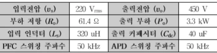
cos 0 -250 -500 250 500 0 0.02 0.04 Time (s) 0 -40 -80 40 80 vo [V] v s [V] isx5 [A] 0 100 200 300 400 500 vdec [V] vdec_ref [V] idec [A] idec_ref [A] time [s] 그림4 APD회로PSIM시뮬레이션 결과Fig. 4 PSIM simulation result of APD circuit.
max
≥ × max
≤
≤
cos35
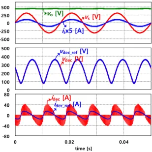
-0 -250 -500 250 500 0 100 200 300 400 500 0 0.02 0.04 Time (s) 0 -40 -80 40 80 vo [V] vs [V] isx5 [A] vdec[V] vdec_ref [V] idec [A] idec_ref [A] time [s] 그림 5 제안하는 기법이 적용된APD회로 시뮬레이션 결과 Fig. 5 Simulation result of APD circuit with proposed method.
×
cos
Δ
max min
Δ
제어부 Totem-pole PFC APD 회로 그림6검증 실험을 위한 프로토타입Fig. 6 Prototype for experimental verification.
is (50A/div.) vs (200V/div.) vo (200V/div.) 5ms/div 5ms/div vdec (200V/div.) idec(50A/div.) 그림 7검증 실험 결과
Fig. 7 Experimental verification result. 표 2제안한 기법을 통한APD회로 설계 결과
Table 2 Design result of APD circuit based on proposed method.