Demonstration of photonics-aided terahertz
wireless transmission system with using silicon
photonics circuit
S
ANG-R
OKM
OON,
1S
EUNGJUNH
AN,
2S
ANGHWAY
OO,
1H
EUKP
ARK,
1W
ON-K
YOUNGL
EE,
1J
OONK
IL
EE,
1J
ONGWOOP
ARK,
2K
YOUNGSIKY
U,
2S
EUNG-H
YUNC
HO,
1 ANDJ
OONYOUNGK
IM3,*1Optical Network Research Section, Electronics and Telecommunications Research Institute (ETRI), 218 Gajeong-ro, Yuseong-gu, Daejeon, 34129, South Korea
2School of Electrical Engineering, Korea Advanced Institute of Science and Technology (KAIST), 291 Daehak-ro, Yuseong-gu, Daejeon, 34141, South Korea
3Department of Information and Communications Engineering, Sangmyung University, 31 Sangmyungdae-gil, Dongnam-gu, Cheonan-si, 31066, South Korea
Abstract: We experimentally demonstrate the use of silicon photonics circuit (SPC) in the
simple and cost-effective photonics-aided Terahertz (THz) wireless transmission system. We perform theoretical investigation (with experimental confirmation) to understand that the system performance is more sensitive to the free space path loss (FSPL) at the THz wireless link than the SPC’s insertion loss. The SPC, we design and fabricate, combines two incident optical carriers at different wavelengths and modulates one of two optical carriers with data to transfer, consequently reducing the system footprint that is indeed one of the key challenges that must be tackled for better practicability of the THz communication system. We perform experimental verification to show the feasibility of 40 Gb/s non-return-to-zero (NRZ) on-off-keying (OOK) signal transmission over 1.4 m wireless link for possibly its application in short-reach indoor wireless communication systems utilizing (sub-)THz frequency band such as, e.g., indoor WiFi, distributed antenna/radio systems, rack-to-rack data delivery, etc. The SPC could be further integrated with various photonic elements such as semiconductor optical amplifiers, laser diodes, and photo-mixers, which will enable the path towards all-photonic THz-wave synthesizers.
© 2020 Optical Society of America under the terms of theOSA Open Access Publishing Agreement
1. Introduction
(Sub-)Terahertz (THz) windows are gaining rising interests from telecommunications community thanks to its inherently advantageous properties such as broad bandwidth (at least tens of GHz) over a huge unlicensed spectral range [1–5]. The recent world radiocommunication conference (WRC) dealt with Agenda Item 1.15 that considers 275-450 GHz spectrum for land-mobile and fixed services applications [6]. For example, the spectrum at 300 GHz between water-absorption peaks could be considered for diverse initiatives such as kiosk downloading, ultra-high speed indoor WiFi, rack-to-rack data interconnect, mobile backhaul, next-generation mobile network (e.g., 6G), etc. [2–6]. In response to these trends, the electronics is putting a lot of efforts into developing high-speed transceivers (TRx) and amplifiers based on silicon or III-V semiconductor technologies [7–11]. Recently, the SiGe Heterojunction Bipolar Transistor (HBT) technology enabled 220-260 GHz TRx that is able to deliver 81 Gb/s 64QAM signal over 1 m distance [9]. At slightly higher frequency (285-315 GHz) the InGaAs mHEMT technology realized the THz TRx, demonstrating 56 Gb/s signal transmission over 10 m. For achieving that long reach (i.e., 10 m), large antenna gain of 72 dBi and heterodyning technique were exploited [10]. Moreover,
#398460 https://doi.org/10.1364/OE.398460
diverse photonics-inspired devices such as photonic-crystal waveguides, multiplexers, filters, modulators, and so on were proposed in the past decade to close the THz gap [11].
The THz-waves, in spite of such abundant spectrum, imply multiple limitations. The first is the ultra-large line-of-sight (LOS) path loss that limits the wireless reach to be a couple of meters without the electrical amplification at the THz band or ultra-large gain (e.g. 50 dBi) antennas. More importantly, the THz-waves do not propagate through the most of building materials, and have poor diffraction capabilities, leading the cell size to be much smaller (i.e., the number of cells to be much bigger) than the current wireless systems (e.g., LTE, 5G, etc.). As such, it is crucial to secure the technical tools to bring the THz-wave based services indoor where over 80% of wireless data is being consumed [12]. Thus, one could make use of photonics technology which is being actively adopted in the mobile network for its seamless and efficient integration with modern radio access network using, e.g., analog/digital radio-over-fiber technologies, etc. [12,13]. The optical-wireless convergence networks provide the distribution of wireless signals throughout specific geometric area, where the fiber-optic cabling is utilized between the hub-units and the remote access units (RAU). At the RAU, the THz-signal can be generated based on optical heterodyning with ultra-large bandwidth photo-mixers such as unitravelling carrier-photodiode (UTC-PD) or electro-optic plasmonic modulator [1,2,14–16]. The avoidance of using multiple electronic devices (such as mixers, oscillators, multi-stage frequency-multipliers, etc. at THz-band) would simplify and lighten the architecture of the RAUs, of which is a great number indeed, making the system more efficient and flexible in terms of implementation and reconfiguration, potentially reducing the cost as well.
In recent years, there have been a lot of diverse efforts from the photonics society to adopt the optical technology in the THz wireless communication system, gradually enhancing the performance, i.e., the BL product (where B is the bit-rate and L is the wireless distance) [15–21]. The limiting factor is too-low output power of THz emitters (i.e., photo-mixers), which is normally on the order of tens of micro-Watts [1,2]. Until now the best performance was achieved by T. Harter et al., demonstrating feasibility to transfer 100 Gb/s data over 100 m through the simultaneous use of low-noise amplifiers (LNA) and power amplifiers (PA) at 300 GHz region [18]. Also, the total capacity was leveraged by the multi-input and multi-output (MIMO) scheme based in wavelength/polarization multiplexing [19]. Furthermore, digital signal processing (DSP) techniques such as, e.g., probabilistic shaping, nonlinear distortion compensation, etc. were applied for compensating the signal distortions due to the imperfect transfer function of the optical-THz links [20]. More recently, C. Castro et al. demonstrated the real-time QPSK transmission, realizing the THz-wireless fiber extender to bridge the bypass-area where the fiber-optic cabling is not available [21].
The aforementioned photonics-aided THz wireless communication systems, however, are formed by using many different sorts of photonic elements such as optical sources, electro-optic modulators, optical couplers, optical attenuators, etc. that eventually need to be integrated in order to reduce the footprint and energy consumption, etc. As such, the photonic integration is being considered to be one of the most critical missions to realize more practical THz communication systems [2]. Recently, G. Carpintero et al. utilized the InP-Polymer dual tunable lasers injection-locked to the external optical frequency comb to generate the frequency-stabilized THz wave at 330 GHz, demonstrating 18 Gb/s NRZ signal transmission with external optical modulators and the UTC-PD [22]. In addition, E. Lacombe et al. demonstrated 10 Gb/s NRZ transmission over 0.3 meters THz link at 300 GHz using the photo-mixer produced with the industrial silicon photonics technology that offers multiple advantages [23]. Silicon photonics, being more specific, is compatible with industrial CMOS technologies, which enables high volume production for low cost per device [24]. Furthermore, it provides high index contrast between the core and cladding of waveguide, allowing for large-scale and high-complexity integration [24].
In this paper, for the first time to the best of our knowledge, we design and experimentally demonstrate the silicon-based photonic integrated circuit for optical modulation and coupling in the THz communication system. One of main concerns about utilizing the silicon photonics circuit (SPC) in the THz system is that the SPC will cause a significant optical attenuation, consequently degrading signal transmission performance: i.e., the signal-to-noise ratio (SNR). Thus, prior to the photonic circuit design, we investigate the dependence of the THz system performance on the optical attenuation induced by the SPC. And then we design the SPC with which replaces the multiple devices such as modulators and optical passive components and patch cords. Following the characterization of each key element (i.e. silicon modulator and UTC-PD) of our system, we measure the normalized gain of the THz wireless link. And then we experimentally demonstrate the THz wireless communication system at 300 GHz that allows for the transmission of tens of Gb/s on-off keying (OOK) signals. The SPC contains the modulator and passive components at the moment, though it could possibly be a platform for further integration with more diverse optical devices. For example, it may be further integrated with optical sources. Additionally, since the photonic THz system requires heavy optical amplification prior to the photo-mixers, the SPC could be integrated with semiconductor optical amplifiers (SOA).
2. Design of THz wireless link and silicon photonics circuit (SPC)
When it comes to the limiting factors of the THz system performance, the main challenge concerns two aspects: i) THz-wave signal power (e.g., ∼tens of µW at the UTC-PD output), and ii) the free space path loss (FSPL) at the THz link (e.g., 81.9 dB for 1 m transmission at 300 GHz). Thus, one may consider making use of THz amplifiers at the output of the UTC-PD and/or at the THz receiver side even though the THz amplifiers are still below the commercial requirements [11,18]. Another option could be to apply the phased array antenna architecture to the THz transmitter [25].
In addition, a significant optical attenuation by the SPC might further degrade the system performance as well, which is indeed one of top concerns raised when embedding the SPC in the THz wireless communication system. As such, we investigate the impacts of insertion loss of the SPC on the THz system performance. The baseband SNR (abbreviated SNRBB) of the THz
wireless communication system can be expressed as follow [1,3]:
SNRBB =
SBB
NTHz_Tx+ NTHz_Rx
(1)
where, SBB, NTHz_Tx, and NTHz_Rxrepresent the received baseband signal, noise attribution from
the THz-Tx, and noise of the THz-Rx, respectively, at the output of the THz-Rx. Each term can be expressed as follows:
SBB= PS_THz_TxGAnt_TxGAnt_RxGLens2/(LFSPLLconv) (2)
NTHz_Tx= PN_THz_TxGAnt_TxGAnt_RxGLens2/(LFSPLLconv) (3)
NTHz_Rx= NSDThNFAmpB (4)
where LFSPLis the FSPL that is obtained by (4πdfc/c)2, where d is wireless distance, fcis carrier
frequency and c is the speed of light. In Eq. (2) and (3), PS_THz_Txand PN_THz_Txindicate the
signal and noise power generated by the UTC-PD, where the SNR (i.e., PS_THz_Tx/PN_THz_Tx) can
be expressed as [26]:
SNRTHz_Tx = ((SNRRIN)−1+ (SNRsig−spon−beat)−1)−1 (5)
where SNRRINand SNRsig_spon_beatrepresent the SNR caused by the relative intensity noise (RIN)
amplifier. These terms can be represented as:
SNRRIN= m/(2B × RINLaser) (6)
SNRsig_spon_beat = mPEDFA_in/(8nsphνB) (7)
where m is modulation depth, which is 0.5 when two optical carriers are identical in power, and nspand h are spontaneous emission factor and Planck constant, respectively. The
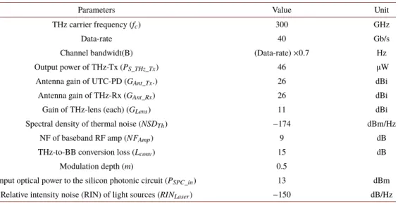
thermal-and shot-noise terms were omitted under the assumption that the received optical power is high enough (e.g., >11 dBm in our system) to be the optical noise (i.e., RIN and SSBN)-limited system. Table1summarizes the parameters to derive the baseband SNR (SNRBB) of the THz
system. The parameter values were obtained from the experimental system we built for this work. The input optical power to the EDFA (PEDFA_in) is represented as PSPC_in/LSPC, where PSPC_in
and LSPCare optical input power to the SPC and optical attenuation by the SPC, respectively.
Table 1. Simulation parameters
Parameters Value Unit
THz carrier frequency (fc) 300 GHz
Data-rate 40 Gb/s
Channel bandwidt(B) (Data-rate) ×0.7 Hz
Output power of THz-Tx (PS_THz_Tx) 46 µW
Antenna gain of UTC-PD (GAnt_Tx.) 26 dBi
Antenna gain of THz-Rx (GAnt_Rx) 26 dBi
Gain of THz-lens (each) (GLens) 11 dBi
Spectral density of thermal noise (NSDTh) −174 dBm/Hz
NF of baseband RF amp (NFAmp) 9 dB
THz-to-BB conversion loss (Lconv) 15 dB
Modulation depth (m) 0.5
Input optical power to the silicon photonic circuit (PSPC_in) 13 dBm
Relative intensity noise (RIN) of light sources (RINLaser) −150 dB/Hz
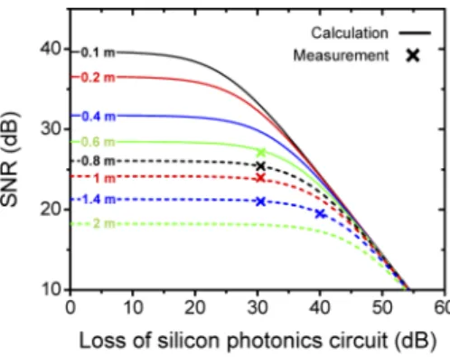
Figure 1 shows the calculated baseband SNR (i.e., SNRBB) as a function of the optical
attenuation due to the SPC (i.e., LSPC) at various wireless distances in comparison to the
measurement results. In the calculation, as shown in Table1, we assume that the THz output power and the total THz antenna/lens gain are fixed at 46 µW and 74 dBi, respectively, without considering the use of THz-amplifiers or phased antenna arrays. We also assume that the SPC loss is fully compensated by optical amplifiers, maintaining the constant THz output power. Thus, as the SPC loss (LSPC) is increasing, the noise of the received THz signal (i.e., NTHz_Tx, in Eq. (1)
and (3)) is increased. However, when the FSPL (see LFSPLin Eq. (3)) is much larger than the
THz antenna/lens gain (e.g., 74 dBi in our case), the noise of the received THz signal (NTHz_Tx)
would be highly attenuated to be smaller than the THz-Rx noise (NTHz_Rx), consequently NTHz_Rx
becoming the dominant system limiting factor. For example in Fig.1, if the wireless distance is 2 meters (where the LFSPLis 87.9 dB), the SNR does not decrease till the SPC loss becomes larger
than 35 dB since the SNRBBis determined by the THz-Rx noise. On the other hand, for short
distance such as 0.1 meters (where the LFSPLis 61.9 dB), NTHz_Txwould be larger than NTHz_Rxin
Eq. (1). If this is the case, the effect of increase in the SPC loss (LSPC) will be more visible as seen
in Fig.1. Thus, for some indoor applications such as, e.g., 6G distributed antenna/radio system, WiFi, rack-to-rack interconnects, etc., where the simple RAU architecture and relatively short distances are required, the SPC insertion loss may not exceed 30 dB. In case the THz-amplifiers
Fig. 1. Signal-to-noise ratio (SNR) as a function of the optical attenuation by the silicon
photonics circuit for various wireless distances.
are utilized to compensate the FSPL, insertion loss requirement of the SPC will be stricter as compared to the case with no THz-amplifiers used.
Following the analysis, we designed the SPC that consists of two arms that guide two optical beams at different wavelengths as illustrated in Fig.2(a). One of two arms comprises an intensity modulator for signal-modulation, while the other arm just adjusts the power of the continuous wave (CW) optical carrier. In the photonic circuit, two optical beams (one is modulated while the other is not) are coupled and then sent towards the photo-mixer (the UTC-PD in our system) that leads to the beat of two optical carriers (at different wavelengths), consequently generating the THz-wave signal.
Fig. 2. (a) Schematic diagram of the silicon photonics circuit and (b) the cross-section
structure of silicon-based series push-pull Mach-Zehnder modulator (MZM).
The key element of the silicon photonics circuit is the travelling wave (TW)-type series push-pull Mach-Zehnder modulator (MZM), its cross-section structure depicted in Fig.2(b). Each phase arm, which is formed by the P-N junction at the center of the rib waveguide, consists of 4 regions that have different width and doping concentration levels. We inserted N+ and P+ regions for making Ohmic contacts. The doping levels of N and P regions were set to be 1.8 × 1018 cm−3 and 1.3 × 1018 cm−3, respectively. The length of the modulator was 2 mm
that provides an acceptable combination of insertion loss and modulation bandwidth. The π-phase shift was achieved at 10 V reverse voltage. To achieve impedance matching and identical transmission speed of electrical signal to that of light-wave throughout the silicon waveguide, we optimized the transmission line structures. We fabricated the SPC through domestic open-access foundry.
Figure3shows the normalized EO frequency response (up-to 50 GHz) of the silicon MZM for two different bias voltages applied to the P+ region via metal contact#2 (M2 in Fig.2(b)). At the bias of 0 V, the 3 dB modulation bandwidth was measured to be ∼15 GHz. As decreasing the bias down to −4 V, the 3 dB modulation bandwidth was enlarged to 35 GHz. We see the clearly-open
eye-diagram at −4 V bias where the modulation speed was 26.5 Gb/s. The extinction ratio was 7.9 dB when the applied peak-to-peak voltage was set to be 4.5 V.
Fig. 3. Measured modulation characteristic, i.e., electro-optic (EO) response, of the silicon
Mach-Zehnder modulator (MZM).
3. Experimental setup and results
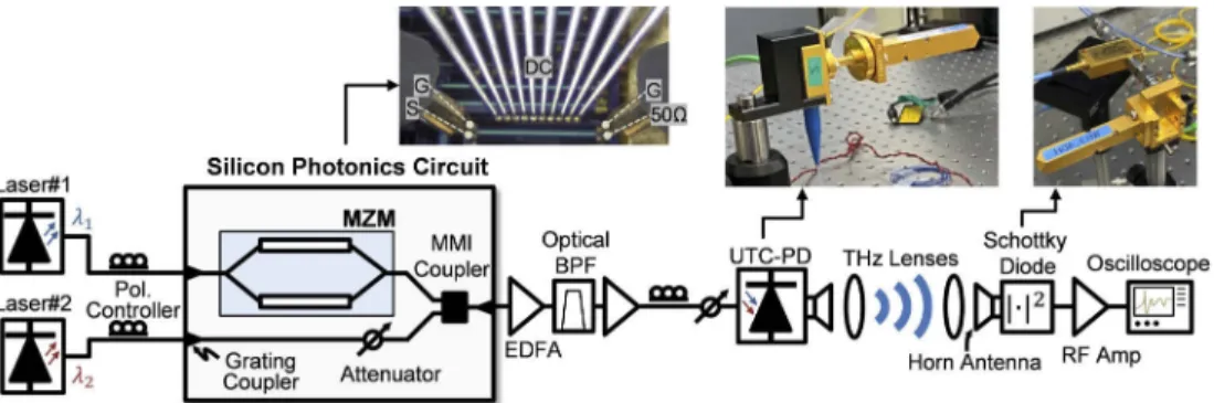
In this section, we carry out the experimental demonstration of the SPC in the simple and cost-effective THz wireless communication system based on the intensity-modulation/direct-detection (IM/DD) scheme as seen in Fig.4. For this, we utilize two optical sources: one (N7711A, Keysight) for the data transfer, which is “Laser#1” at 1535 nm (10 dBm), and the other (8164B, Agilent) operating in CW mode for the optical beating, which is “Laser#2” at 1537.4 nm (6 dBm). Two laser outputs are injected to the SPC via silicon grating couplers. The optical carrier at 1535 nm passes by the series push-pull MZM that is driven with non-return-to-zero (NRZ) signals. During the experiment, we keep the electrical peak-to-peak voltage to be ∼6 V, and vary the bit-rate from 25 to 40 Gb/s which was limited by our lab capability. The RF (NRZ) signal and DC bias (−4 V) are applied to the metal contacts via the RF and DC probes on high-precision stages.
Fig. 4. Experimental setup of the THz wireless communication system using silicon
photonics circuit (SPC).
In the experiment, the SPC induced ∼30 dB optical attenuation on the optical carrier (at 1535 nm). The SPC loss includes two grating couplers (9.2 dB), multimode interference (MMI) couplers (0.8 dB), MZM (9 dB including the modulation loss), bending/rib-to-channel losses (0.3 dB), and routing path (10.1 dB where the routing length was >2 cm). Thus, the optical attenuation could be reduced by more than ∼10 dB through further improvement of circuit design, i.e., by shortening the routing path length and employing H2 thermal annealing process. The
lower arm of the photonic circuit includes the variable optical attenuator, which is indeed an interferometer using an electrical current-driven heater, so as to adjust the optical carrier at 1537.4 nm to be same power as that of the data-carrying optical signal at the output of the MMI coupler, which leads to the optimum SNR of the generated THz signal. The total optical power at the output of the silicon photonics circuit was measured to be about −17 dBm. To compensate the insertion loss of the SPC, we employed a couple of Erbium-doped fiber amplifiers (EDFA). The output optical power of the 1stEDFA was ∼8 dBm. The OBPF, which is to filter out the amplified spontaneous emission (ASE) noise, attenuates the optical power to ∼3 dBm that is the input optical power to the 2ndEDFA. The output power of the 2ndEDFA (i.e., ∼20 dBm) is then adjusted by the variable optical attenuator (VOA) in order to adjust the input optical power to the UTC-PD.
Figure5shows the measured optical spectrum after the cascaded EDFAs. The optical SNR (OSNR) was about 38 dB at 0.1 nm resolution bandwidth, which could be further improved by reducing the insertion loss of SPC, subsequently, removing one of two EDFAs as well. Note that, however, the 38 dB OSNR does not result in distinct degradation of the transmission performance as the limiting factor of the THz communication system is the huge attenuation at the wireless link, as discussed in Fig.1.
Fig. 5. Measured optical spectrum after two cascaded EDFAs.
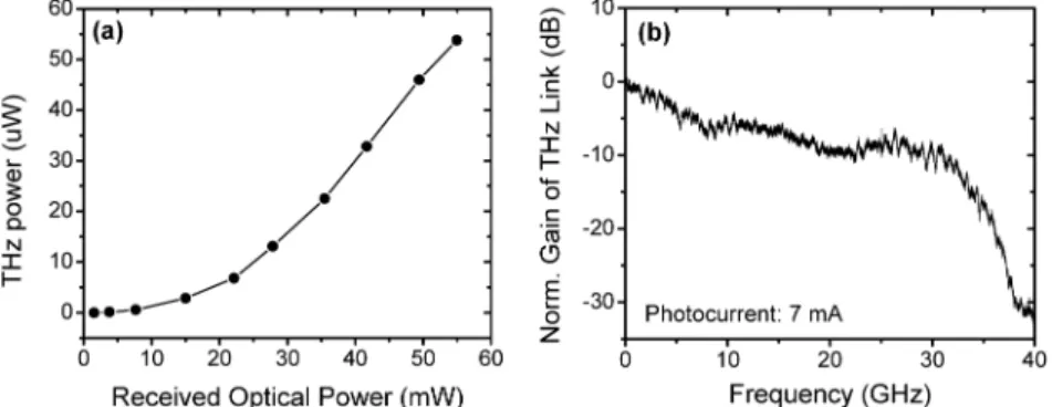
Upon the reception of the optical signal, the UTC-PD produces the NRZ-OOK signal carried by the THz wave at the frequency as same as the difference between the data-carrying optical signal and the CW light (i.e. ∼300 GHz). Firstly, we measured the power of generated THz signal with using a THz power-meter (Erickson PM5, Virginia Diodes) as varying the received optical power. For this, we placed the THz power-meter in close proximity (∼0.5 cm) to the UTC-PD’s WR3.4 horn antenna. The THz power was varied from 0 to 46 µW when increasing the received optical power up-to 55 mW (that corresponds to the DC photocurrent up-to 7.5 mA), as seen in Fig.6(a). Within the measurement range in Fig.6(a), the responsivity of the UTC-PD at DC was measured to be ∼0.14 A/W.
In order to guide the signal towards the THz receiver, we used a couple of THz lenses (that have 10 cm focal length) that partly compensate the FSPL (i.e., 84.8 dB for 1.4 m at 300 GHz) [1,2]. The THz receiver consists of the horn antenna (WR3.4) followed by the Schottky barrier diode detector (ZBD-F, Virginia Diodes) and the broadband RF amplifier (> 40 GHz). The use of Schottky barrier diode, which is a square law detector, down-converting the THz signal to baseband, simplifies the system configuration and management especially when compared to coherent systems that include THz mixers and local oscillators that ideally need to be frequency/phase-locked to the oscillator at the central unit. Figure6(b) shows the normalized gain of the THz link centered at 300 GHz that includes the THz-Tx (i.e., UTC-PD and horn-antenna), THz-lenses, wireless link, THz-Rx (i.e., horn-antenna, Schottky barrier diode, and the RF amplifier). For the measurement, Laser#1 was replaced by the spectrum-sliced ASE
Fig. 6. (a) Measured THz power at the output of the UTC-PD vs received optical power
and (b) the normalized gain of the THz wireless link at 300 GHz.
light source where its center frequency was set as same as Laser#1. As seen in Fig.6(b), the THz link’s response falls by 6 dB at ∼17 GHz when compared to DC, which would be enough for transmission of >25 Gb/s signals.
Finally, we characterized the bit-error-rate (BER) performance of the SPC-based THz wireless communication system. We captured the THz-receiver’s output signal with using the real-time oscilloscope for the following DSP and BER calculation. The DSP includes two steps: i) a low-pass filter (LPF) and ii) a decision feedback equalizer (DFE). At the LPF step, a Bessel filter was utilized, where its bandwidth was 0.7 times the data-rate, which is known to be the optimum bandwidth ratio in typical NRZ-OOK transmission system. For the DFE step, we used 2 × 10⁴
training symbols where each symbol has 2 samples. Based on the experiment, we optimized the number of taps to be 35 for forward and 1 for backward directions.
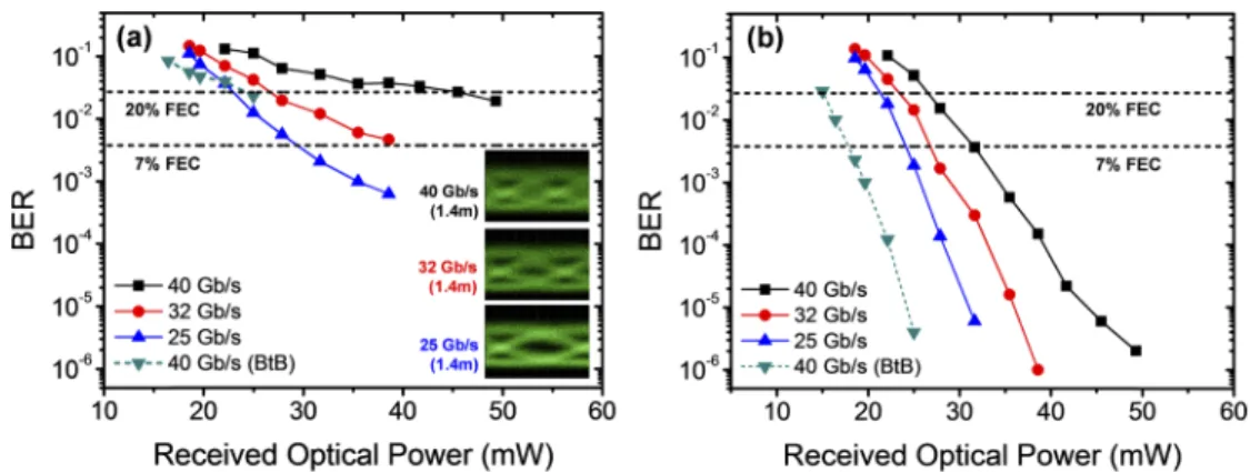
We repeated the experiment at three different data-rates (25, 32, and 40 Gb/s), varying the received optical power at the UTC-PD from 15 to 49.3 mW (i.e., varying the photocurrent from 2 to 7 mA). Note that the output power of the SPC and the EDFAs were not changed during the measurement. Instead, we utilized the VOA to adjust the input optical power to the UTC-PD. The PRBS pattern length was 215-1 and the wireless distance was fixed at 1.4 m. Firstly, we investigate the BER performance without the offline DSP (i.e., the LPF only) that implies a simple implementation of the system at the expense of the performance. As seen in Fig.7(a), the THz system meets the 20% FEC requirement for the data-rate up-to 40 Gb/s. For the 7% FEC, we achieve the transmission of up-to 32 Gb/s. As the inset eye-diagrams indicate, the system performance was limited by the bandwidth as well as the noise that could be resolved with using the DFE that would not lead to the significant increase of system complexity. Subsequently, it was possible to meet the BER requirements of the 7% FEC for all the three data-rates, see Fig.7(b). To be more specific, when the data-rate was 40 Gb/s the BER was measured to be 2×10⁻⁶ at the received optical power of 49.3 mW, where the THz output power was 46 µW.
This BER value (2×10⁻⁶) corresponds to the SNR of 19.5 dB which is ∼1.6 dB lower than the theoretical derivation result (i.e., ∼21.1 dB SNR at 1.4 m transmission when the chip loss is 30 dB) shown in Fig.1. This slight mismatch is attributed to two aspects: i) the THz-link is bandwidth-limited system (see Fig.6(b)) in spite of using the DFE, and ii) the extinction ratio was less than 10 dB (i.e., ∼7.9 dB) as shown in Fig.3.
To investigate the available frequency range of our system, we measured the BER with changing the THz-carrier frequency from 230 to 340 GHz as shown in Fig.8. For this, we actually changed the lasing wavelength of the Laser#2. In the experiment, the data-rate and wireless distance were fixed at 40 Gb/s and 1.4 m, respectively. We also show the measured back-to-back (BtB) result for the comparison. Figure8shows the gradual performance improvement as the carrier frequency
Fig. 7. Measured BER values as a function of the received optical power at three different
data-rates (a) without and (b) with the offline digital signal processing (DSP).
is increasing from 230 to 300 GHz. On the other hand, a sudden BER degradation is observed as the frequency increases from 300 to 340 GHz. This is because the horn antenna of the THz receiver is based on the WR3.4 waveguide that has the operation frequency range of 220–320 GHz. The Schottky barrier diode used in the experiment also has the largest responsivity at around 300 GHz. Figure8indicates that the operation frequency range would be >70 GHz.
Fig. 8. Measured BER performances as a function of the carrier frequency at 40 Gb/s and
1.4 m.
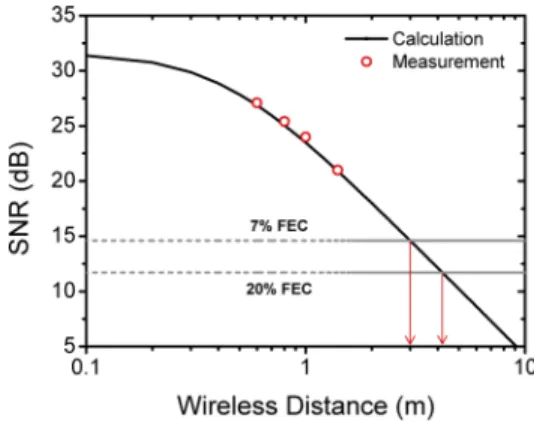
In our experiment, the wireless distance was limited to 1.4 meters due to the constraint of the experimental setup. Thus, we further investigate the available maximum wireless distance of our system through the SNR analysis as seen in Fig.9. The simulation parameters were set as same as Table1. The data-rate was 40 Gb/s and the SPC loss was set to be 30 dB which is in line with our BER measurement setup. Figure9shows the SNR as a function of the transmission distance at 40 Gb/s. We also show the level of SNR required for making use of FECs at different overhead ratio (see the dashed gray lines). We observe that our system based on the SPC could be extended up-to 3 meters with the 7% FEC and 4 meters with the 20% FEC, respectively.
Fig. 9. Signal-to-noise ratio (SNR) as a function of wireless distance at 40 Gb/s data-rate
and 30 dB insertion loss of silicon photonics chip.
4. Conclusion
We demonstrated the silicon photonics circuit (SPC) in the Terahertz (THz) wireless communica-tions system. For this, we designed and fabricated the SPC that consists of two photonic arms that can provide two functions: i) combining the optical signal with the optical local oscillator, and ii) optical intensity modulation. For the signal modulation we designed the travelling wave (TW) type series push-pull Mach-Zehnder modulator (MZM) where its modulation bandwidth was measured to be ∼35 GHz at the bias of −4 V. The THz link was established by a photo-mixer and a Schottky barrier diode, supporting a simple and cost-effective intensity-modulation/direct detection (IM/DD) scheme. As a photo-mixer, we exploited the uni-travelling carrier photodiode (UTC-PD) that generated 300 GHz carrier at the output power of 46 µW. The incoherent system would be suitable for indoor applications such as optical-wireless convergence network, where the wireless signals are distributed to a great number of remote units that is required to have simple architecture for high flexibility and efficiency. Although the SPC induced ∼30 dB attenuation on the optical signals (partly due to the long routing path length), the THz wireless communications system was able to provide 40 Gb/s signal transmission over 1.4 m. Such large insertion loss of the SPC could be reduced through multiple improvement of the silicon chip design and fabrication. Firstly, the fiber coupling loss could be relieved utilizing advanced grating coupler design technologies such as apodization and silicon overlaying, or other fiber coupling schemes such as end-fire coupling and adiabatic coupling. The excess waveguiding loss (10.1 dB) could be highly reduced by shorting the length and employing H2 thermal annealing process which can make silicon sidewalls smooth. The insertion loss of phase shifters also can be enhanced while maintaining the modulation efficiency by doping profile optimization. The limiting factor of our system, indeed, was the free space path loss (FSPL) rather than the insertion loss of the SPC. Nevertheless, for indoor short-reach applications in which the FSPL is relatively small, the SPC would need to have as low insertion loss as possible (e.g., <30 dB). The SPC would be possibly providing additional integration with other photonic elements such laser diodes, semiconductor optical amplifiers, and PDs.
Disclosures
The authors declare no conflicts of interest.
References
1. A. J. Seeds, H. Shams, M. J. Fice, and C. C. Renaud, “TeraHertz Photonics for Wireless Communications,”J. Lightwave Technol.33(3), 579–587 (2015).
2. T. Nagatsuma, G. Ducournau, and C. C. Renaud, “Advances in terahertz communications accelerated by photonics,” Nat. Photonics10(6), 371–379 (2016).
3. A.-A. A. Boulogeorgos, A. Alexiou, T. Merkle, C. Schubert, R. Elschner, A. Katsiotis, P. Stavrianos, D. Kritharidis, P.-K. Chartsias, J. Kokkoniemi, M. Juntti, J. Lehtomäki, A. Teixeira, and F. Rodrigues, “Terahertz Technologies to Deliver Optical Network Quality of Experience in Wireless Systems Beyond 5G,”IEEE Commun. Mag.56(6), 144–151 (2018).
4. V. Petrov, J. Kokkoniemi, D. Moltchanov, J. Lehtomäki, Y. Koucheryavy, and M. Juntti, “Last Meter Indoor Terahertz Wireless Access: Performance Insights and Implementation Roadmap,”IEEE Commun. Mag.56(6), 158–165 (2018). 5. H.-J. Song, H. Hamada, and M. Yaita, “Prototype of KIOSK Data Downloading System at 300 GHz: Design,
Technical Feasibility, and Results,”IEEE Commun. Mag.56(6), 130–136 (2018).
6. M. J. Marcus, “WRC-19 Issues: Agenda Item 1.15 and the Use of 275–450 GHz,”IEEE Wirel. Commun.23(6), 2–3 (2016).
7. M. H. Eissa, A. Malignaggi, R. Wang, M. Elkhouly, K. Schmalz, A. C. Ulusory, and D. Kissinger, “Wideband 240-GHz Transmitter and Receiver in BiCMOS Technology With 25-Gbit/s Data Rate,”IEEE J. of Solid-State Circuits53(9), 2532–2542 (2018).
8. S. Lee, S. Hara, T. Yoshida, S. Amakawa, R. Dong, A. Kasamatus, J. Sato, and M. Fujishima, “An 80-Gb/s 300-GHz-Band Single-Chip CMOS Transceiver,”IEEE J. of Solid-State Circuits54(12), 3577–3588 (2019). 9. P. Rodriguez-Vazquez, J. Grzyb, B. Heinemann, and U. R. Pfeiffer, “Optimization and Performance Limits of a
64-QAM Wireless Communication Link at 220-260 GHz in a SiGe HBT Technology,” IEEE Radio and Wireless
Symposium(2019).
10. I. Dan, G. Ducournau, S. Hisatake, P. Szriftgiser, R.-P. Braun, and I. Kallfass, “A Superheterodyne 300 GHz Wireless Link for Ultra-Fast Terahertz Communication Systems,” 49th European Microwave Conference (EuMC) (2019). 11. K. Sengupta, T. Nagatsuma, and D. M. Mittleman, “Terahertz integrated electronic and hybrid electronic–photonic
systems,”Nat. Electron.1(12), 622–635 (2018).
12. J. Kim, M. Sung, S.-H. Cho, Y.-J. Won, B.-C. Lim, S.-Y. Pyun, J.-K. Lee, and J. H. Lee, “MIMO-Supporting Radio-Over-Fiber System and its Application in mmWave-Based Indoor 5G Mobile Network,”J. Lightwave Technol. 38(1), 101–111 (2020).
13. M. Sung, J. Kim, E.-S. Kim, S.-H. Cho, Y.-J. Won, B.-C. Lim, S.-Y. Pyun, J.-K. Lee, and J. H. Lee, “RoF-based Radio Access Network for 5G Mobile Communication Systems in 28 GHz Millimeter-wave,”J. Lightwave Technol. 38(2), 409–420 (2020).
14. A. Melikyan, L. Alloatti, A. Muslija, D. Hillerkuss, P. C. Schindler, J. Li, R. Palmer, D. Korn, S. Muehlbrandt, D. Van Thourhout, B. Chen, R. Dinu, M. Sommer, C. Koos, M. Kohl, W. Freude, and J. Leuthold, “High-speed plasmonic phase modulators,”Nat. Photonics8(3), 229–233 (2014).
15. Y. Salamin, B. Baeuerle, W. Heni, F. C. Abrecht, A. Josten, Y. Fedoryshyn, C. Haffner, R. Bonjour, T. Watanabe, M. Burla, D. L. Elder, L. R. Dalton, and J. Leuthold, “Microwave plasmonic mixer in a transparent fibre–wireless link,” Nat. Photonics12(12), 749–753 (2018).
16. S. Ummethala, T. Harter, K. Koehnle, Z. Li, S. Muehlbrandt, Y. Kutuvantavida, J. Kemal, P. Marin-Palomo, J. Schaefer, A. Tessmann, S. K. Garlapati, A. Bacher, L. Hahn, M. Walther, T. Zwick, S. Randel, W. Freude, and C. Koos, “THz-to-optical conversion in wireless communications using an ultra-broadband plasmonic modulator,”Nat. Photonics13(8), 519–524 (2019).
17. K. Liu, S. Jia, S. Wang, X. Pang, W. Li, S. Zheng, H. Chi, X. Jin, X. Zhang, and X. Yu, “100 Gbit/s THz Photonic Wireless Transmission in the 350-GHz Band With Extended Reach,”IEEE Photonic Tech. L.30(11), 1064–1067 (2018).
18. T. Harter, C. Fullner, J. N. Kemal, S. Ummethala, M. Brosi, E. Bründermann, W. Freude, S. Randel, and C. Koos, “110-m THz Wireless Transmission at 100 Gbit/s Using a Kramers-Kronig Schottky Barrier Diode Receiver,” 2018
European Conference on Optical Communication (ECOC)T3F.7 (2018).
19. X. Li, J. Yu, K. Wang, M. Kong, W. Zhou, Z. Zhu, C. Wang, M. Zhao, and G.-K. Chang, “120 Gb/s Wireless Terahertz-Wave Signal Delivery by 375 GHz-500 GHz Multi-Carrier in a 2 × 2 MIMO System,”J. Lightwave Technol.37(2), 606–611 (2019).
20. X. Li, J. Yu, L. Zhao, W. Zhou, K. Wang, M. Kong, G.-K. Chang, Y. Zhang, X. Pan, and X. Xin, “132-Gb/s Photonics-Aided Single-Carrier Wireless Terahertz-Wave Signal Transmission at 450GHz Enabled by 64QAM Modulation and Probabilistic Shaping,” Optical Fiber Communication Conference 2019, M4F.4 (2019).
21. C. Castro, R. Elschner, T. Merkle, C. Schubert, and R. Frenud, “100 Gb/s Real-Time Transmission over a THz Wireless Fiber Extender Using a Digital-Coherent Optical Modem,” Optical Fiber Communication Conference 2020, M4I.2 (2020).
22. G. Carpintero, S. Hisatake, D. Felipe, R. Guzman, T. Nagatsuma, and N. Keil, “Wireless Data Transmission at Terahertz Carrier Waves Generated from a Hybrid InP-Polymer Dual Tunable DBR Laser Photonic Integrated Circuit,” Sci. Rep.8(1), 3018 (2018).
23. E. Lacombe, C. Belem-Goncalves, C. Luxey, F. Gianesello, C. Durand, D. Gloria, and G. Ducournau, “10-Gb/s Indoor THz Communications Using Industrial Si Photonics Technology,”IEEE Microw. Wirel. Co.28(4), 362–364 (2018).
24. W. Bogaerts and L. Chrostowski, “Silicon photonics circuit design: methods, tools and challenges,”Laser Photonics Rev.12(4), 1700237 (2018).
25. H. Kanaya, K. Tsugami, G. Sakano, G. C. Eu, and K. Kato, “Development of 4 ( 4 phased array antenna on chip for 300GHz band application,”Proc. SPIE10531, 1053114 (2018).
26. E.-S. Kim, J. Kim, M. Sung, S.-H. Cho, and J. H. Lee, “Power budget improvement of multi-IFoF based analog indoor-distributed antenna system (DAS) with laser over-modulation,”Opt. Commun.435, 129–133 (2019).