ICCAS2005 June 2-5, KINTEX, Gyeonggi-Do, Korea
1. INTRODUCTION
The need for voltage elevators has increased with the apparition of circutis operating from single battery cell. But their principle does not allow a high level of efficiency in standard CMOS technologies. The growing portable equipment has made a strong demand for low voltage operation in EEPROMs. Although a minimum power supply voltage of 2.1V has been achieved in previously reported, further improvements in an on chip high voltage generator circuit are indispensable to obtain a power supply voltage below 2 V. This article discusses the theoretical low-voltage limit of the conventional high-voltage generator, Dickson’s charge pump circuit, and describes the design of a charge pump circuit applicable of power supply as low as 1 V by using the CMOS circuit without body effect of the device.
2. CONVENTIONAL CHARGE PUMP CIRCUIT
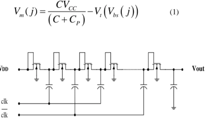
The conventional Dicson charge pump circuit shown in figure 1 the voltage gained at jth stage Vm(j) is given by(
)
(
( )
)
( )
CC m t PCV
V
j
V V
j
C
C
=
−
+
bs (1)Fig. 1. Conventional Dickson’s charge pump circuit where C and CP are clock coupling capacitance and parasitic
capacitance at the input node (Cgs of the devices) of each unit
stage, respectively, VCC is the clock amplitude equal to the
power supply voltage, and Vt (Vbs(j)) represents the threshold
voltage of the jth nMOS transistor with a substrate bias of Vbs(j).
Equation (1) indicates that as the output voltage of each stage increases, Vm(j) decreases due to the body effect. When the
threshold voltage of the last stage’s transistor becomes equal to the CVCC/(C+Cp), the output voltage is not increased by the
addition of subsequent stages. As C is much larger than CP in
typical conditions, the maximum output voltage VMAX obtained
by a conventional charge pump is given by
A New Analog Switch CMOS Charge Pump Circuit without Body Effect
Jirawath Parnklang, Ampual Manusphrom, Nut Laowanichpong ,
and Narongchai Tongnoi
Department of Electronic Faculty of Engineering, King Mongkut’s Institute of Technology Ladkrabang, Bangkok, Thailand (Tel : +66-2-326-0643; E-mail: [email protected])
Abstract: The charge – pump circuit which is used to generate higher voltage than the available supply voltage has wide applications
such as the flash memory of EEPROM Because the demand for high voltage comes from physical mechanism such as the oxide tunneling, the required pumped voltage cannot be scaled as the power supply voltage is scaled. Therefore, an efficient charge – pump circuit that can achieve high voltage from the available low supply voltage is essential. A new Analog Switch p-well CMOS charge pump circuit without the MOS device body effect is processed. By improve the structure of the circuit’s transistors to reduce the threshold voltage shift of the devices, the threshold voltage of the device is kept constant. So, the circuit electrical characteristics are higher output voltage within a shorter time than the conventional charge pump. The propose analog switch CMOS charge pump shows compatible performance of the ideal diode or Dickson charge pump.
Keywords: MOSFET Circuit, Body Effect, Charge Pump
2 0
2
2
CC t MAX F FV
V
V
φ
φ
γ
⎛
−
⎞
=
⎜
+
⎟
−
⎝
⎠
(2)where Vt0 is the zero-bias threshold voltage, γ is the body
effect coefficient, and φF is the substrate’ s Femi potential.
3. PROPOSE CHARGE PUMP CIRCUIT
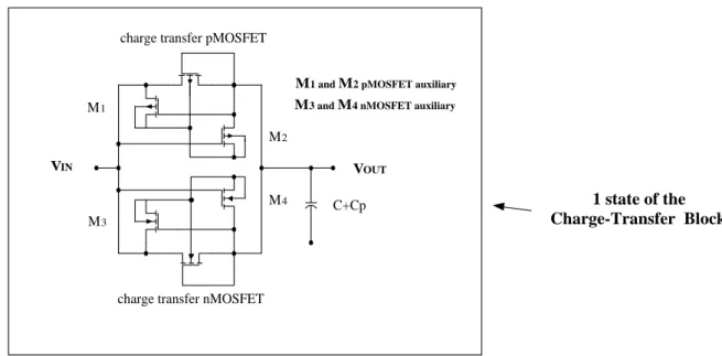
To generate a sufficient programming voltage with such a small power supply voltage, we propose a charge pump circuit, in which the voltage gained at each stage is not degraded by the body effect of the deviceThe proposed charge pumps shown by the schematic in the figure 2. Two auxiliary MOSFET of each side are introduced to control the body bias. The source side auxiliary MOSFET shares the source and the gate with the charge- transfer MOSFET and the drain side auxiliary MOSFET shares the drain with the charge-transfer MOSFET. For each charge-transfer block, two auxiliary MOSFET’s and one charge-transfer MOSFET share the body, which is separated from the body of other block. For the positive Pumping, the proposed circuit is composed of only pMOSFET’s so that it can be made compact with little possibility of the latchup. When the charge-transfer MOSFET is ON, the source side auxiliary MOSFET always turns on. Then the source and the body of the charge-transfer MOSFET are connected through the source side auxiliary MOSFET, so that no reverse bias exists between the source and the body of the charge-transfer MOSFET preventing threshold voltage increase. When the charge–transfer MOSFET is OFF, the drain side auxiliary MOSFET turns on so that the drain and the body of the charge-transfer VDD clk clk Vout
212
ICCAS2005 June 2-5, KINTEX, Gyeonggi-Do, Korea
VIN VOUT
C+Cp
charge transfer nMOSFET charge transfer pMOSFET
M1
M2
M4
M3
M1 and M2 pMOSFET auxiliary M3 and M4 nMOSFET auxiliary
1 state of the
Charge-Transfer Block
Figure 2. One block of the propose charge pump MOSFET are connected to prevent the body from floating.
When the clk is low and the clk is high, the jth charge-transfer
MOSFET is ON and charges are transferred through it. At this moment, the source side auxiliary MOSFET of the jth charge-transfer MOSFET turn on so that the source and the body of the jth charge-transfer MOSFET are connected. In this
way, regardless of the pumped voltage, the threshold voltage of the jth charge-transfer MOSFET stays with Vto (the
threshold voltage at zero back bias) during the charge transfer state. In this clock state, the (j-1)th charge-transfer MOSFET is OFF and the drain side auxiliary MOSFET. When the clk is high and the clk is low, the proposed pump operates in the same manner as the previous state.
To verify the circuit concept, SPICE program is used for all of the simulation. The 3 state of each charge pump (Dickson and the propose charge pump) have 5pF load capacitor and the clk voltage is 5 V . The output voltage of each charge pump have shown in figure 3
Figure 3(A) 3 state Dickson Charge Pump
Figure 3(B) 3 state Propose Charge Pump
Figure 3(C) 5 state Dickson Charge Pump
ICCAS2005 June 2-5, KINTEX, Gyeonggi-Do, Korea
Figure 3(D) 5 state Propose Charge Pump
The output voltage of the propose charge pump with 3 state and 5 state have even higher output voltage than the conventional Dickson charge pump.
4. CONCLUSION
A new charge pump has been present by controlling the body voltage of the charge-transfer device. It has been shown that much higher output voltage than the Dickson charge pump is obtained by the newly proposed charge pump with variable body voltage. With two auxiliary MOSFET’s of each side, the body voltage is adjusted to remove the threshold voltage increase. By the SPICE simulation, it has been shown that the proposed charge pump successfully follows the performance of the ideal diode charge pump.
ACKNOWLEDGMENTS
The authors gratefully acknowledge the contribution of Dr. Warakorn Kaseamsuwan . The best lecturer in analog IC design of the department.
REFERENCES
[1] Ph. E. Allen and D. R. Holberg, “CMOS Analog Circuit Design”, Saunders, 1987
[2] K. Martin, “Digital Integrated Circuit design” Oxford, 2000
[3] J. Wu and K. Chang, “MOS Charge Pumps for Low – Voltage Operation” IEEE J. Solid-State Circuit, vol.33, no. 4, pp. 592 – 597, April 1998.
[4] L. J. Stotts, “Introduction to Implantable Biomedical IC Design” IEEE Circuits and Devices Magazine, pp 12 – 18 , Jan. 1989
[5] M. Steyaert J. Crols, S. Gogaert and W. Sansen, “ Low – voltage Analog CMOS filter Design” IEEE Proc.
ESCAS-93 Chicago Illinois, pp. 1447-1450, May 1993